Zxld1352, Block diagram, Pin description – Diodes ZXLD1352 User Manual
Page 2
ZXLD1352
ZXLD1352
Document number: DS33469 Rev. 3 - 2
2 of 21
December 2010
© Diodes Incorporated
A Product Line of
Diodes Incorporated
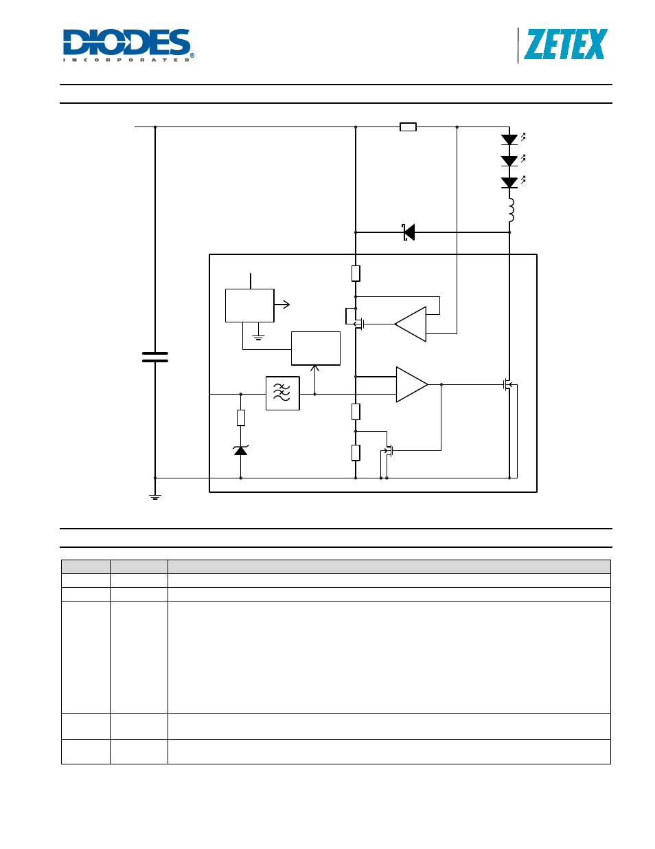
Block Diagram
Figure 1. Block Diagram
Pin Description
Name
Pin No.
Description
LX
1
Drain of NDMOS switch
GND 2
Ground
(0V)
ADJ 3
Multi-function On/Off and brightness control pin:
• Leave floating for normal operation. (V
ADJ
= V
REF
=1.25V giving nominal average output current
I
OUTnom
=0.1/R
S
)
• Drive to voltage below 0.2V to turn off output current ADJ <2.5V) to adjust output current from 25% to 200% † of I OUTnom • Drive with PWM signal from open-collector or open-drain transistor, to adjust output current. o Adjustment range 0.1% to 100% of I OUTnom for 100Hz < f < 1kHz • Connect a capacitor from this pin to ground to define soft-start time. Soft-start time is approx.0.5ms/nF) I SENSE 4 Connect resistor R S from this to V IN to define nominal average output current I OUTnom =0.1/R S (Note: R SMIN =0.27V with ADJ pin open circuit) V IN 5 Input voltage (7V to 30V). Decouple to ground with 1µF of higher X7R ceramic capacitor close to MN - + V IN Comparator R1 R2 R3 GND - + LX V IN I SENSE Current sense circuit V IN ADJ R S L1 D1 5V Voltage Shutdown Vref 50k 1.25V 600KHz C1
• Drive with DC voltage (0.3V
device
regulator
circuit