Zxld1352, Application information – Diodes ZXLD1352 User Manual
Page 13
ZXLD1352
ZXLD1352
Document number: DS33469 Rev. 3 - 2
13 of 21
December 2010
© Diodes Incorporated
A Product Line of
Diodes Incorporated
Application Information
(Continued)
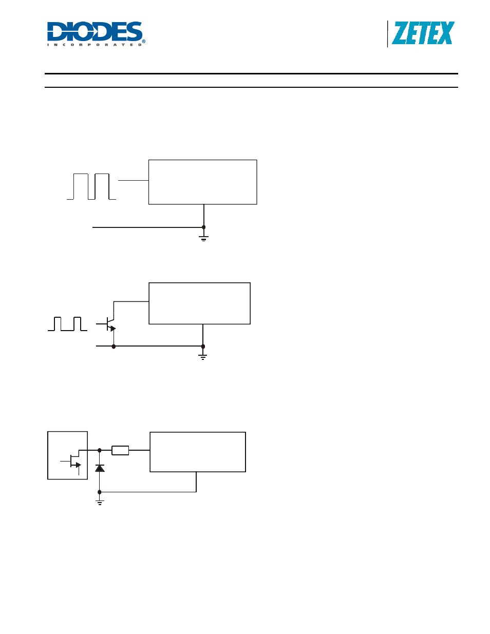
Output Current Adjustment by PWM Control
Directly driving ADJ input
A Pulse Width Modulated (PWM) signal with duty cycle D
PWM
can be applied to the ADJ pin, as shown below, to adjust the
output current to a value above or below the nominal average value set by resistor R
S
:
Driving the ADJ input via open collector transistor
The recommended method of driving the ADJ pin and controlling the amplitude of the PWM waveform is to use a small NPN
switching transistor as shown below:
This scheme uses the 50k resistor between the ADJ pin and the internal voltage reference as a pull-up resistor for the external
transistor eg MMBT3904.
Driving the ADJ input from a microcontroller
Another possibility is to drive the device from the open drain output of a microcontroller. The diagram below shows one method
of doing this:
If the NMOS transistor within the microcontroller has high Gate / Drain capacitance, this arrangement can inject a negative spike
into ADJ input of the ZXLD1352 and cause erratic operation but the addition of a Schottky clamp diode (eg Diodes Inc.
SD103CWS) to ground and inclusion of a series resistor (3.3k) will prevent this. See the section on PWM dimming for more
details of the various modes of control using high frequency and low frequency PWM signals.
PWM
GND
0V
V
ADJ
GND
ZXLD1352
ADJ
GND
ZXLD1352
ADJ
MCU
10k
PWM
GND
ZXLD1352
ADJ
GND