Zxsc300 – Diodes ZXSC300 User Manual
Page 5
ZXSC300
ISSUE 4 - SEPTEMBER 2007
5
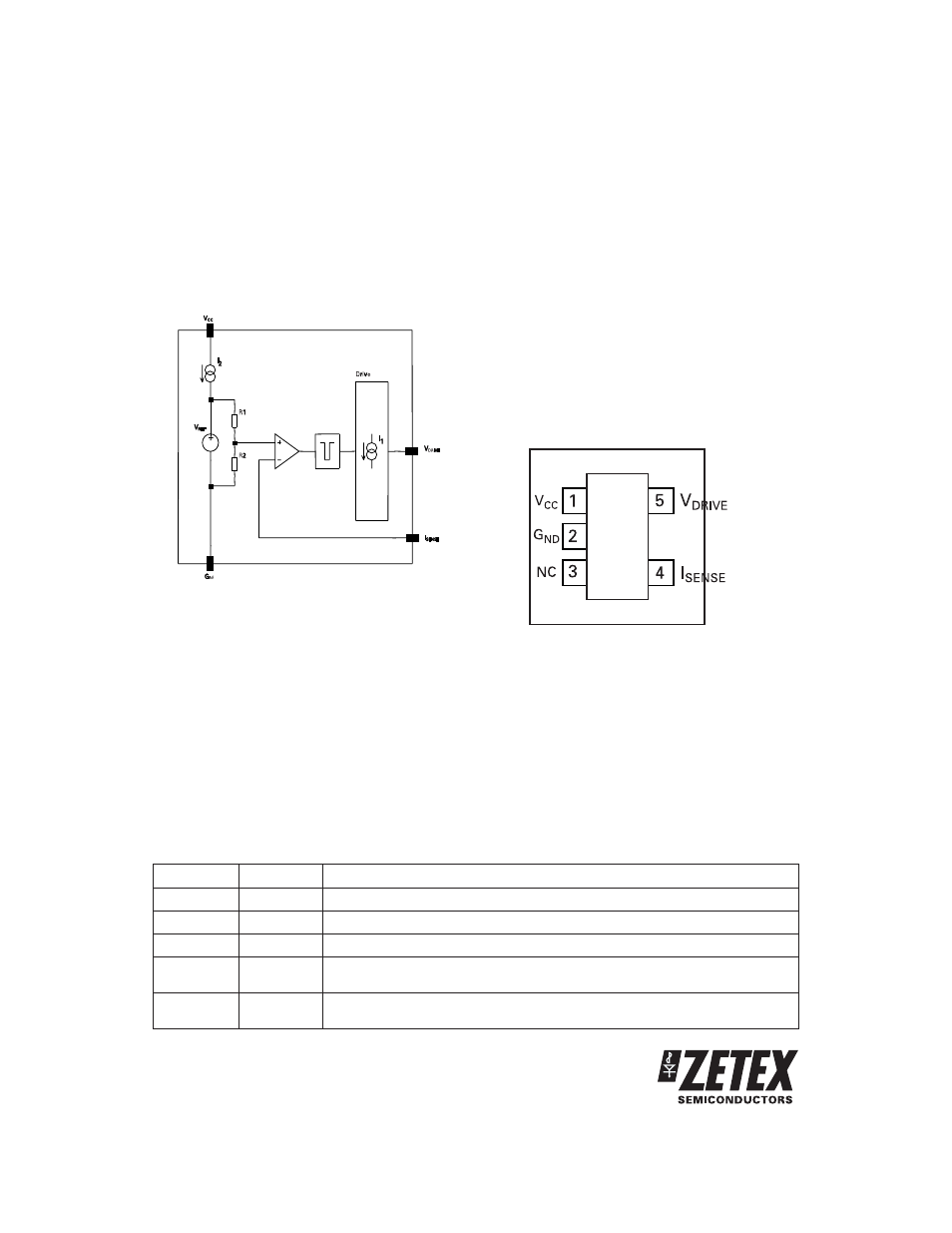
DEVICE DESCRIPTION
The ZXSC300 is
PFM, controller IC which, when
combined with a high performance external transistor,
enables the production of a high efficiency boost
converter for use in single cell LED driving
applications. A block diagram is shown for the
ZXSC300 in Figure 1.
The on chip comparator forces the driver circuit and
therefore the external switching transistor off if the
voltage at I
SENSE
exceeds 19mV. This threshold is set
by an internal reference circuit and divider.
The Voltage at I
SENSE
is taken from a current sense
resistor connected in series with the emitter of the
switching transistor. A monostable following the
output of the comparator forces the turn-off time of the
output stage to be typically 1.7µs. This ensures that
there is sufficient time to discharge the inductor coil
before the next on period.
With every on pulse the switching transistor is kept on
until the voltage across the current-sense resistor
exceeds the threshold of the I
SENSE
input. The on-pulse
length, and therefore the switching frequency, is
determined by the programmed peak current, the
input voltage and the input to output voltage
differential. See applications section for details.
The Driver circuit supplies the external switching
transistor with a fixed drive current. To maximise
efficiency the external transistor switched quickly,
typically being forced off within 30ns.
Figure 1 ZXSC300 Block Diagram
Pin Descriptions
Pin No.
Name
Description
1
V
CC
Supply voltage, generally Alkaline, NiMH or NiCd single cell
2
Gnd
Ground
3
N/C
Not connected
4
I
SENSE
Inductor current sense input. Internal threshold voltage set to 19mV.
Connect external sense resistor
5
V
DRIVE
Drive output for external switching transistor. Connect to base of external
switching transistor
Pinout Diagram