Zxsc300 – Diodes ZXSC300 User Manual
Page 2
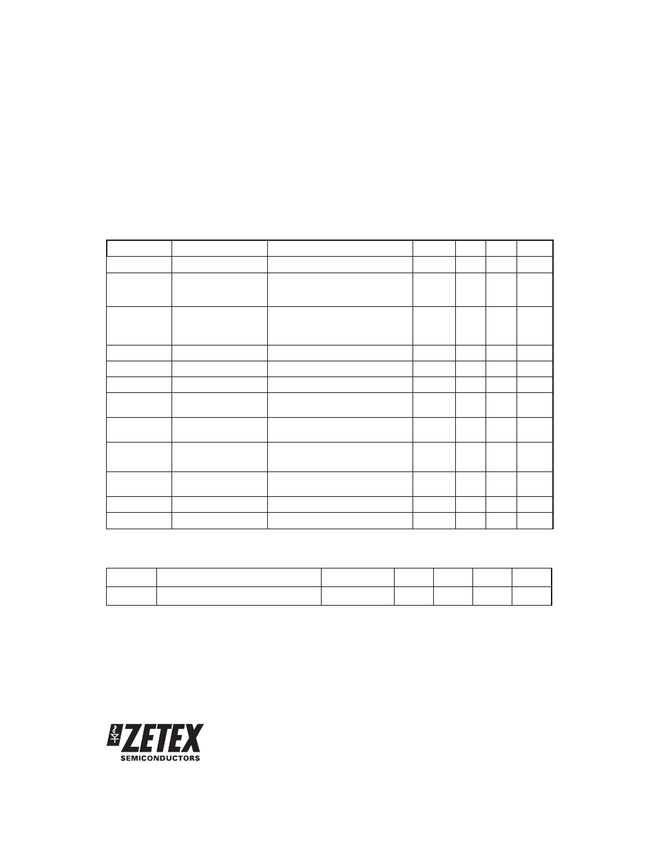
ABSOLUTE MAXIMUM RATING
ZXSC300
ISSUE 4 - SEPTEMBER 2007
2
Supply Voltage
-0.3 to 10V
Maximum Voltage Other Pins -0.3 to V
CC
+0.3V
Power Dissipation
450mW
Operating Temperature
-40 to 85°C
Storage Temperature
-55 to 150°C
ELECTRICAL CHARACTERISTICS: Test conditions unless otherwise stated: V
CC
=1.5V, T
AMB
=25°C
SYMBOL
PARAMETER
CONDITIONS
MIN.
TYP.
MAX.
UNITS
η
Efficiency
(1)
94
%
V
CC
Recommended
supply voltage range
0.8
8
V
V
CC(min)
Minimum startup
and operating
voltage
I
DRIVE
=-600µA, V
DRIVE
=0.7V
I
DRIVE
=-600µA, V
DRIVE
=0.7V,
T
AMB
=-10°C
(3)
0.8
0.9
0.92
V
I
Q
Quiescent current
(2)
0.2
mA
I
VDRIVE
Base drive current
V
DRIVE
= 0.7V, V
ISENSE
= 0V
1.5
3.6
mA
I
CC
Supply current
(3)
V
DRIVE
= 0.7V, V
ISENSE
= 0V
2
4
mA
V
VDRIVE(high)
High level drive
voltage
V
ISENSE
= 0V, I
VDRIVE
=-0.5mA
V
CC
-0.3
V
CC
V
V
VDRIVE(low)
Low level drive
voltage
V
ISENSE
= 50mV, I
VDRIVE
= 5mA
0
0.2
V
V
ISENSE
(threshold)
Output current
reference voltage
14
19
24
mV
T
CVISENSE
I
SENSE
voltage temp co.
2
0.4
%/°C
I
ISENSE
I
SENSE
input current
V
ISENSE
= 0V
0
-30
-65
µA
T
DRV
Discharge pulse width
1.2
1.7
3.2
µs
SYMBOL
PARAMETER
CONDITIONS
MIN.
TYP.
MAX.
UNITS
F
OSC
Recommended operating frequency
(4)
200
kHz
1
Application dependent, see reference designs.
2
These parameters guaranteed by design and characterisation
3
Total supply current =I
Q
+ I
VDRIVE
, see typical characteristics
4
Operating frequency is application circuit dependent. See applications section.
OPERATING CONDITIONS