Zxld1321, Absolute maximum ratings – Diodes ZXLD1321 User Manual
Page 3
ZXLD1321
Issue 1 - January 2008
3
www.zetex.com
© Zetex Semiconductors plc 2008
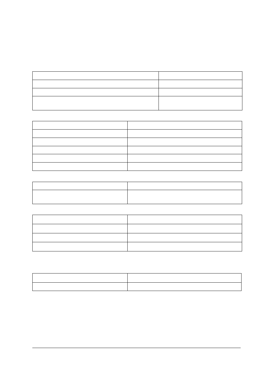
Absolute maximum ratings
(Voltages relative to GND unless otherwise stated)
DC-DC converter
High-side current monitor
Switching NPN transistor
These are stress ratings only. Operation outside the absolute maximum ratings may cause device failure. Operation at the
absolute maximum ratings for extended periods may reduce device reliability.
Thermal resistance
Operating temperature (top)
-40 to 125
°
C
Storage temperature (Tst)
-55 to 150
°
C
Junction temperature (Tj)
-40 to 150
°
C
Package power dissipation (Ptot)
DFN-14 with exposed pad: 4mmx3mm, 0.5mm Pitch
1.5W at Tamb = 70
°
C
Supply voltage (VIN)
-0.3V to +12V
ADJ
-0.3V to The lower of (+5.0V) or (VIN + 0.3V)
CFB
-0.3V to The lower of (+5.0V) or (VIN + 0.3V)
ISENSE
-0.3V to The lower of (+5.0V) or (VIN + 0.3V)
TADJ
-0.3V to The lower of (+5.0V) or (VIN + 0.3V)
BIAS
-0.3V to The lower of (+5.0V) or (VIN + 0.3V)
Monitor supply voltage (M_VIN)
-0.3V to +18V
Continuous sense voltage
(M_VIN – M_LOAD)
-0.3V to +5V
Collector-Base voltage (V
CBO
)
18V
Collector-Emitter voltage (V
CEO
)
18V
Peak pulse current (I
CM
)
3A (Pulse width = 300µs. Duty cycle<=2%)
Continuous Collector current (I
C
)
2A
Junction to case (R
⍜
JC
)
Nominal value
DFN-14
26.3°C/W