Electrical characteristics – Diodes TB0640M - TB3500M User Manual
Page 3
TB0640M - TB3500M
Document number: DS30361 Rev. 10 - 2
3 of 6
November 2011
© Diodes Incorporated
TB0640M - TB3500M
Electrical Characteristics
@T
A
= 25°C unless otherwise specified
Part Number
Maximum
Rated
Repetitive
Off-State
Voltage
Maximum
Off-State
Leakage
Current @
V
DRM
Maximum
Breakover
Voltage
Maximum
On-State
Voltage
@ I
T
= 1A
Breakover
Current
I
BO
Holding Current
I
H
Typical
Off-State
Capacitance
Marking
Code
V
DRM
(V)
I
DRM
(uA)
V
BO
(V)
V
T
(V)
Min
(mA)
Max
(mA)
Min
(mA)
Max
(mA)
C
O
(pF)
TB0640M 58
5
77 3.5
50
800
150
800
140 T064M
TB0720M 65
5
88 3.5
50
800
150
800
140 T072M
TB0900M 75
5
98 3.5
50
800
150
800
140 T090M
TB1100M 90
5
130 3.5
50
800
150
800 90 T110M
TB1300M 120
5
160 3.5 50
800
150
800 90 T130M
TB1500M 140
5
180 3.5 50
800
150
800 90 T150M
TB1800M 160
5
220 3.5 50
800
150
800 90 T180M
TB2300M 190
5
265 3.5 50
800
150
800 60 T230M
TB2600M 220
5
300 3.5 50
800
150
800 60 T260M
TB3100M 275
5
350 3.5 50
800
150
800 60 T310M
TB3500M 320
5
400 3.5 50
800
150
800 60 T350M
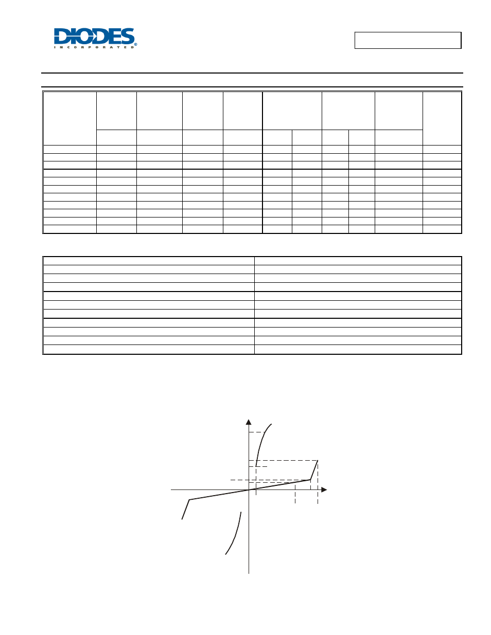
Symbol Parameter
V
DRM
Stand-off Voltage
I
DRM
Leakage current at stand-off voltage
V
BR
Breakdown voltage
I
BR
Breakdown current
V
BO
Breakover voltage
I
BO
Breakover current
I
H
Holding current Note 4
V
T
On state voltage
I
PP
Peak pulse current
C
O
Off-state capacitance Note 5
Notes: 4.
I
H
> (V
L
/R
L
) If this criterion is not obeyed, the TSPD triggers but does not return correctly to high-resistance state. The surge recovery time does not
exceed 30ms.
5. Off-state capacitance measured at f = 1.0MHz, 1.0V
RMS
signal, V
R
= 2V
DC
bias.
I
BO
V
BR
V
DRM
V
T
V
BO
I
H
I
V
I
BR
I
DRM
I
PP