P-channel typical characteristics –continued, Test circuits, C c apa cit a nc e ( pf) -v – Diodes ZXMHC3F381N8 User Manual
Page 9: Drain - source voltage (v)
ZXMHC3F381N8
Issue 1.0 - March 2009 9
© Diodes Incorporated
P-channel typical characteristics –continued
1
10
0
200
400
600
800
1000
C
RSS
C
OSS
C
ISS
V
GS
= 0V
f = 1MHz
C C
apa
cit
a
nc
e (
pF)
-V
DS
- Drain - Source Voltage (V)
0
5
10
15
0
1
2
3
4
5
6
7
8
9
10
I
D
= 5A
V
DS
= 15V
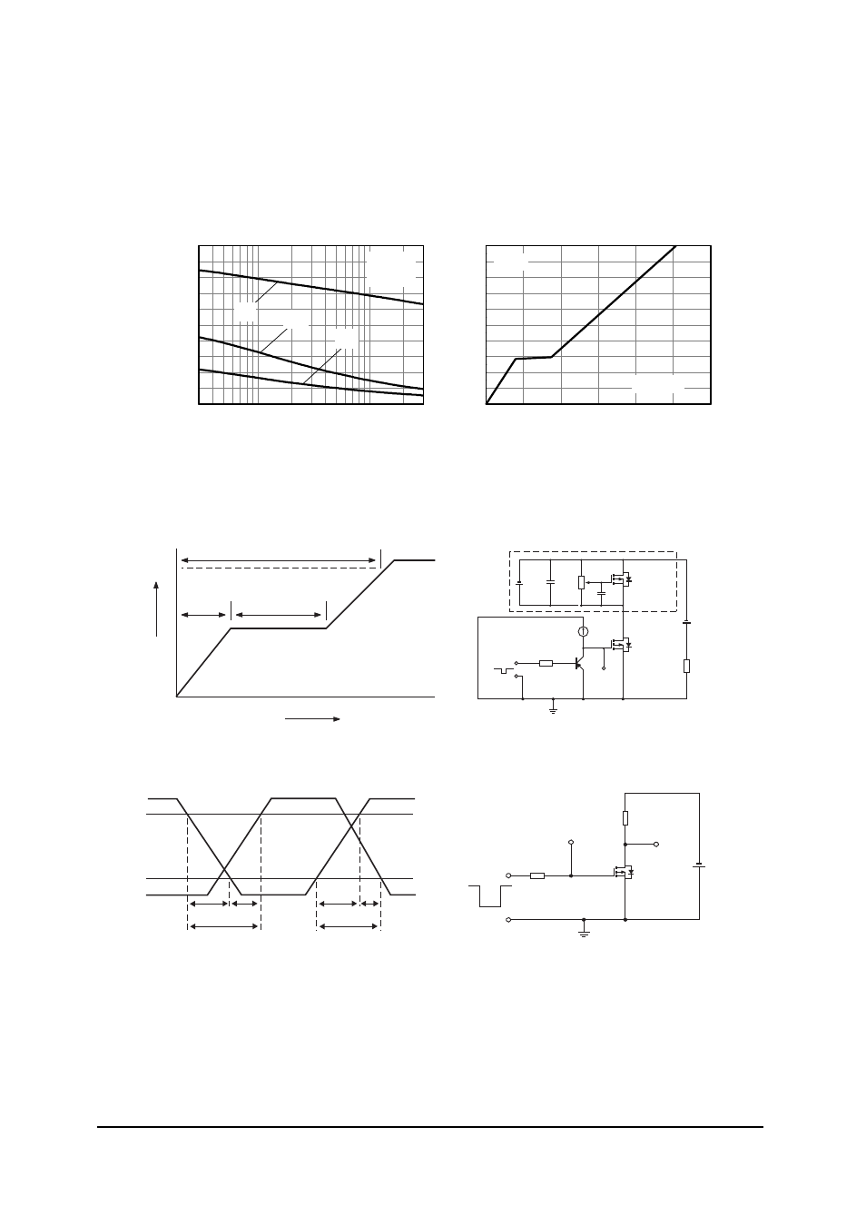
Gate-Source Voltage v Gate Charge
Capacitance v Drain-Source Voltage
Q - Charge (nC)
-V
GS
G
a
te-
S
ourc
e
V
ol
ta
ge (
V
)
Test circuits
Current
regulator
Charge
Gate charge test circuit
Switching time test circuit
Basic gate charge waveform
Switching time waveforms
D.U.T
50k
0.2
F
12V
Same as
D.U.T
V
GS
V
GS
V
DS
V
G
Q
GS
Q
GD
Q
G
V
GS
90%
10%
t
(on)
t
(on)
t
d(on)
t
r
t
r
t
d(off)
V
DS
V
DD
R
D
R
G
Pulse width
Ͻ 1S
Duty factor 0.1%
V
DS
I
D
I
G
See also other documents in the category Diodes Hardware:
- PDS3200 (5 pages)
- PDS340 (5 pages)
- PDS340Q (5 pages)
- PDS360 (5 pages)
- PDS360Q (5 pages)
- PDS4150 (4 pages)
- PDS3100Q (5 pages)
- PDS3100 (5 pages)
- PDS1240CTL (5 pages)
- PDS1045 (5 pages)
- PDS1040L (5 pages)
- PDS1040CTL (5 pages)
- PDS1040 (5 pages)
- PD3S230L (5 pages)
- PD3S230H (3 pages)
- PDS5100Q (5 pages)
- PDS835L (5 pages)
- PDS760 (5 pages)
- PDS560 (5 pages)
- PDS540 (5 pages)
- PDS5100H (5 pages)
- PDS5100 (5 pages)
- PDS4200H (6 pages)
- SBL3060CTP (4 pages)
- SBL30L30CT (3 pages)
- SBL3045CTP (4 pages)
- SBL3040CTP (4 pages)
- SBL2060CTP (4 pages)
- SBL2030CT - SBL2060CT (3 pages)
- SBL2045CTP (4 pages)
- SBL1060CTP (4 pages)
- SBL1040CTP (4 pages)
- SBG3030CT - SBG3045CT (5 pages)
- SB520 - SB560 (3 pages)
- SB370 - SB3100 (3 pages)
- SB320 - SB360 (3 pages)
- SBR10U100CT (5 pages)
- SBR10U150CT (5 pages)
- SBR10A45SP5 (5 pages)
- SBR1060CT (5 pages)
- SBR1045SP5 (5 pages)
- SBR1045SD1 (4 pages)
- SBR1045D1 (5 pages)
- SBR1045CTL (4 pages)
- SBR1040CT (5 pages)