Diodes ZXMHC3F381N8 User Manual
Page 2
ZXMHC3F381N8
Issue 1.0 - March 2009 2
© Diodes Incorporated
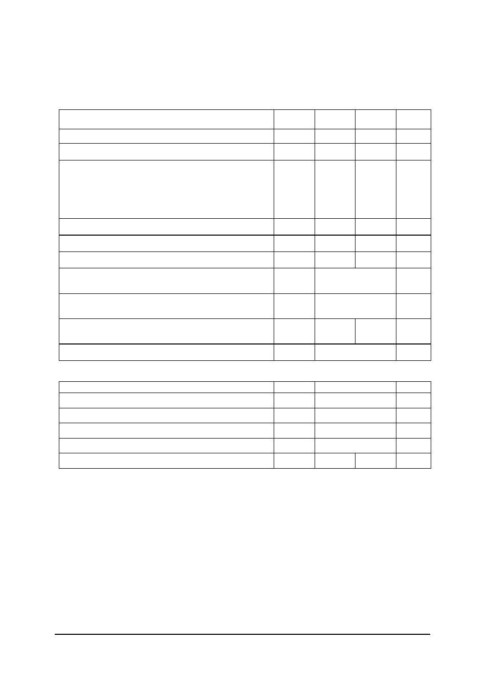
Absolute maximum ratings
Parameter Symbol
N-
channel
P-
channel
Unit
Drain-Source voltage
V
DSS
30 -30 V
Gate-Source voltage
V
GS
±20
±20
V
Continuous Drain current @ V
GS
= 10V; T
A
=25
°C
(b)
@ V
GS
= 10V; T
A
=70
°C
(b)
@ V
GS
= 10V; T
A
=25
°C
(a)
@ V
GS
= 10V; T
L
=25
°C
(f)
I
D
4.98
3.98
3.98
4.17
-4.13
-3.31
-3.36
-3.51
A
Pulsed Drain current @ V
GS
= 10V; T
A
=25
°C
(c)
I
DM
22.9 -19.6 A
Continuous Source current (Body diode) at T
A
=25
°C
(b)
I
S
2.0 -2.0 A
Pulsed Source current (Body diode) at T
A
=25
°C
(c)
I
SM
22.9 -19.6 A
Power dissipation at T
A
=25
°C
(a)
Linear derating factor
P
D
0.87
6.94
W
mW/
°C
Power dissipation at T
A
=25
°C
(b)
Linear derating factor
P
D
1.35
10.9
W
mW/
°C
Power dissipation at T
L
=25
°C
(f)
Linear derating factor
P
D
0.95
7.63
0.98
7.81
W
mW/
°C
Operating and storage temperature range
T
j
, T
stg
-55 to 150
°C
Thermal resistance
Parameter Symbol
Value
Unit
Junction to ambient
(a)
R
θJA
144
°C/W
Junction to ambient
(b)
R
θJA
92
°C/W
Junction to ambient
(d)
R
θJA
106
°C/W
Junction to ambient
(e)
R
θJA
254
°C/W
Junction to lead
(f)
R
θJL
131 128
°C/W
NOTES:
(a) For a device surface mounted on 25mm x 25mm x 1.6mm FR4 PCB with high coverage of single sided 1oz copper, in still
air conditions with the heat-sink split into two equal areas (one for each drain connection); the device is measured when
operating in a steady-state condition with one active die.
(b) Same as note (a), except the device is measured at t
≤ 10 sec.
(c) Same as note (a), except the device is pulsed with D= 0.02 and pulse width 300 µs. The pulse current is limited by the
maximum junction temperature.
(d) For a device surface mounted on 50mm x 50mm x 1.6mm FR4 PCB with high coverage of single sided 2oz copper, in still
air conditions with the heat-sink split into two equal areas (one for each drain connection); the device is measured when
operating in a steady-state condition with one active die.
(e) For a device surface mounted on minimum copper 1.6mm FR4 PCB, in still air conditions; the device is measured when
operating in a steady-state condition with one active die.
(f)
Thermal resistance from junction to solder-point (at the end of the drain lead); the device is operating in a steady-state
condition with one active die.