Absolute maximum ratings, Thermal resistance, Zxms6003g – Diodes ZXMS6003G User Manual
Page 4
ZXMS6003G
© Zetex Semiconductors plc 2007
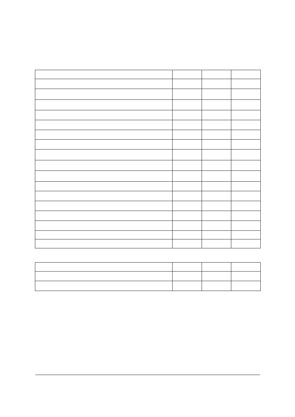
Absolute maximum ratings
NOTES:
(a) For I
D(LIM)
< 1.2A (see safe operating area curve).
(b) For a device surface mounted on 50mm x 50mm x 1.6mm FR4 board with a high coverage of single sided 2oz weight
copper.
(c) For a device surface mounted on FR4 board and measured at t<=10s.
Parameter
Symbol
Limit
Unit
Continuous drain-source voltage
V
DS
60
V
Drain-source voltage for short circuit protection V
IN
V
DS(SC)
36
V
Drain-source voltage for short circuit protection V
IN
=10V
V
DS(SC)
20
V
Continuous input voltage
V
IN
-0.2 ... +10
V
Peak input voltage
V
IN
-0.2 ... +20
V
Operating temperature range
T
j
,
-40 to +150
°C
Storage temperature range
T
stg
-55 to +150
°C
Power dissipation @ T
amb
P
D
2.5
W
Continuous drain current @ V
IN
=10V; T
amb
=25°C
I
D
1.6
A
Continuous drain current @ V
IN
=5V; T
amb
=25°C
I
D
1.4
A
Continuous source current (body diode)
I
S
3
A
Pulsed source current (body diode)
I
S
8
A
Unclamped single pulse inductive energy
E
AS
550
mJ
Load dump protection
V
LoadDump
80
V
Electrostatic discharge (human body model)
V
ESD
4000
V
DIN humidity category, DIN 40 040
E
IEC climatic category, DIN IEC 68-1
40/150/56
Thermal resistance
Parameter
Symbol
Limit
Unit
Junction to ambient
R
⍜JA
50
°C/W
Junction to ambient
R
⍜JA
28
°C/W