Functional block diagram, Applications and information, Zxms6003g – Diodes ZXMS6003G User Manual
Page 2
ZXMS6003G
© Zetex Semiconductors plc 2007
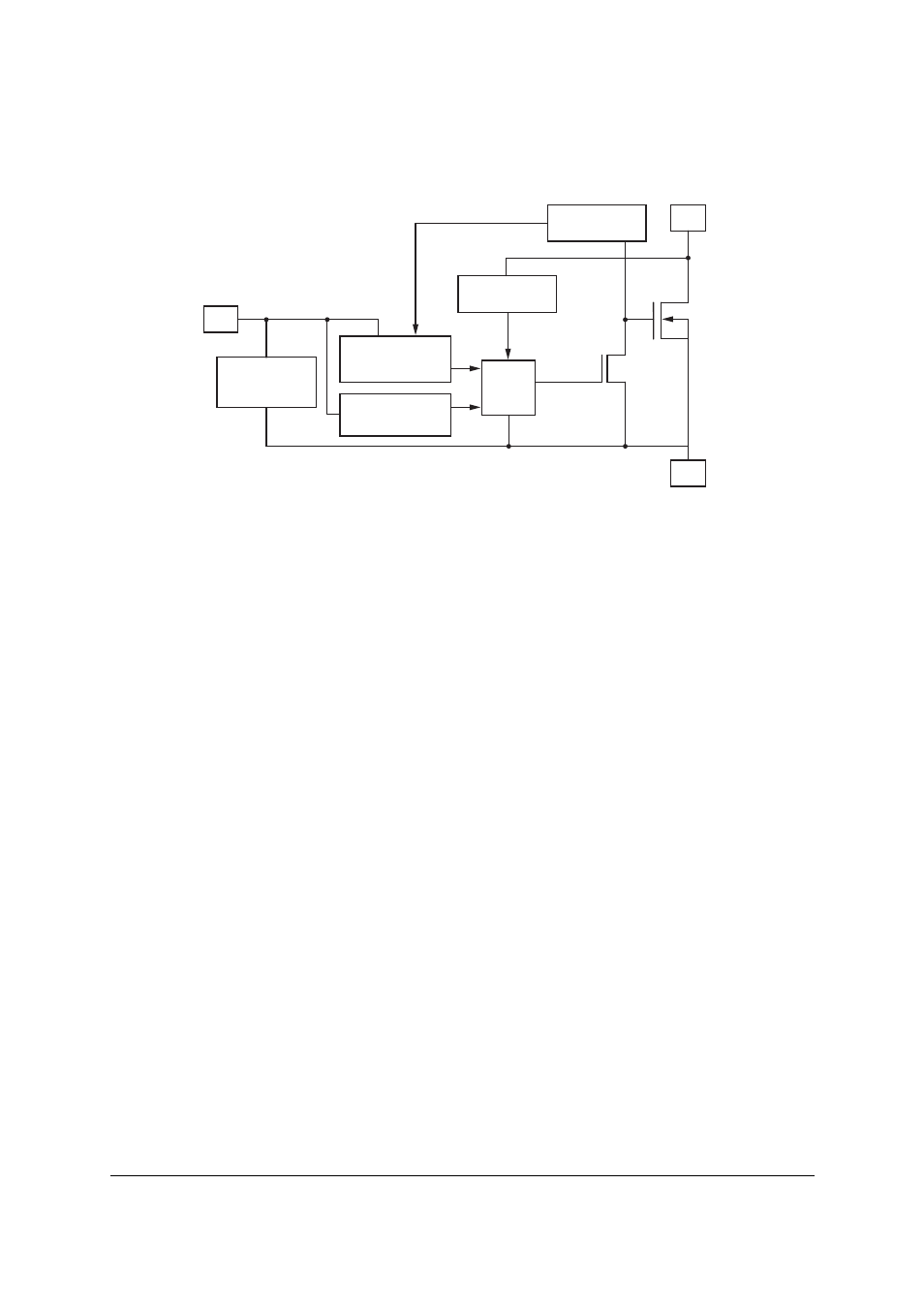
Functional block diagram
Applications and information
•
Especially suited for loads with a high in-rush current such as lamps and motors.
•
All types of resistive, inductive and capacitive loads in switching applications.
•
C compatible power switch for 12V and 24V DC applications.
•
Automotive rated.
•
Replaces electromechanical relays and discrete circuits.
•
Linear mode capability - the current-limiting protection circuitry is designed to de-activate at
low V
DS
, in order not to compromise the load current during normal operation. The design
max. DC operating current is therefore determined by the thermal capability of the package/
board combination, rather than by the protection circuitry.
Note: This does not compromise the product's ability to self-protect during short-circuit load
conditions.
•
The current limit is programmable via an external resistor R
prog
connected between Status and
IN pins.
•
Status pin voltage reflects the gate drive being applied internally to the power MOSFET.
With V
IN
= 5V and R
prog
= 24k
⍀:
Status voltage ~ 5V indicates normal operation.
Status voltage ~ (2-3)V indicates that the device is in current-limiting mode.
Status voltage < 1V indicates that the device is in thermal shutdown.
S
Over voltage
protection
Status /
current limit
Over current
protection
Over temperature
protection
Logic
Human body
ESD protection
D
IN