Zxmc6a09dn8, Thermal resistance, Absolute maximum ratings – Diodes ZXMC6A09DN8 User Manual
Page 2
ZXMC6A09DN8
ISSUE 4 - MAY 2005
2
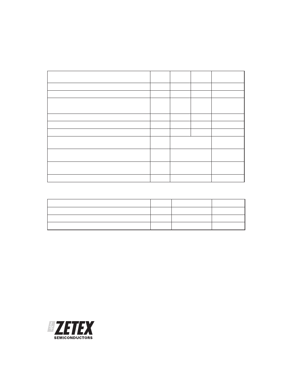
PARAMETER
SYMBOL
VALUE
UNIT
Junction to Ambient
(a)(d)
R
θJA
100
°C/W
Junction to Ambient
(b)(e)
R
θJA
69
°C/W
Junction to Ambient
(b)(d)
R
θJA
58
°C/W
THERMAL RESISTANCE
Notes:
(a) For a dual device surface mounted on 25mm x 25mm x 1.6mm FR4 PCB with high coverage of single sided 1oz copper in still air conditions.
(b) For a dual device surface mounted on FR4 PCB measured at t
Յ10 sec.
(c) Repetitive rating 25mm x 25mm FR4 PCB, D=0.02, pulse width=300µs - pulse width limited by maximum junction temperature.
(d) For a dual device with one active die.
(e) For a device with two active die running at equal power.
PARAMETER
SYMBOL
N-Channe
l
P-Channel
UNIT
Drain-Source Voltage
V
DSS
60
-60
V
Gate-Source Voltage
V
GS
Ϯ20
Ϯ20
V
Continuous Drain Current@V
GS
=10V; T
A
=25
ЊC
(b)(d)
@V
GS
=10V; T
A
=25
ЊC
(b)(d)
@V
GS
=10V; T
A
=25
ЊC
(a)(d)
I
D
5.1
4.1
3.9
-4.8
-3.8
-3.7
A
A
Pulsed Drain Current
(c)
I
DM
25
-23
A
Continuous Source Current (Body Diode)
(b)
I
S
3.5
-3.3
A
Pulsed Source Current (Body Diode)
(c)
I
SM
25.4
-23.8
A
Power Dissipation at T
A
=25°C
(a)(d)
Linear Derating Factor
P
D
1.25
10
W
mW/°C
Power Dissipation at T
A
=25°C
(a)(e)
Linear Derating Factor
P
D
1.8
14
W
mW/°C
Power Dissipation at T
A
=25°C
(b)(d)
Linear Derating Factor
P
D
2.1
17
W
mW/°C
Operating and Storage Temperature Range
T
j
:T
stg
-55 to +150
°C
ABSOLUTE MAXIMUM RATINGS