Zvp4525z, Package dimensions pad layout details – Diodes ZVP4525Z User Manual
Page 9
ZVP4525Z
S E M I C O N D U C T O R S
ISSUE 2 - JUNE 2007
53
Europe
Zetex GmbH
Streitfeldstraße 19
D-81673 München
Germany
Telefon: (49) 89 45 49 49 0
Fax: (49) 89 45 49 49 49
[email protected]
Americas
Zetex Inc
700 Veterans Memorial Hwy
Hauppauge, NY 11788
USA
Telephone: (1) 631 360 2222
Fax: (1) 631 360 8222
[email protected]
Asia Pacific
Zetex (Asia) Ltd
3701-04 Metroplaza Tower 1
Hing Fong Road, Kwai Fong
Hong Kong
Telephone: (852) 26100 611
Fax: (852) 24250 494
[email protected]
Corporate Headquarters
Zetex Semiconductors plc
Zetex Technology Park
Chadderton, Oldham, OL9 9LL
United Kingdom
Telephone (44) 161 622 4444
Fax: (44) 161 622 4446
[email protected]
© Zetex Semiconductors plc 2007
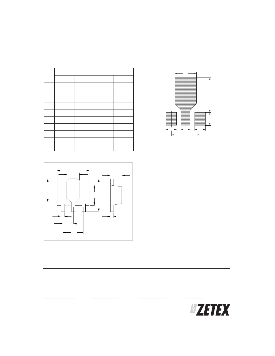
PACKAGE DIMENSIONS
PAD LAYOUT DETAILS
H
A
D B
K
G
N
L
F
C
DIM
Millimetres
Inches
Min
Max
Min
Max
A
4.40
4.60
0.173
0.181
B
3.75
4.25
0.150
0.167
C
1.40
1.60
0.550
0.630
D
-
2.60
-
0.102
F
0.28
0.45
0.011
0.018
G
0.38
0.55
0.015
0.022
H
1.50
1.80
0.060
0.072
K
2.60
2.85
0.102
0.112
L
2.90
3.10
0.114
0.122
N
1.40
1.60
0.055
0.063
1.2
1.0
1.2
3.2
1.5
4.0
2.4
SOT89 pattern.
Minimum Pad Size (dimensions in mm)