Zvp4525z, Electrical characteristics (at t, 25°c unless otherwise stated) – Diodes ZVP4525Z User Manual
Page 4
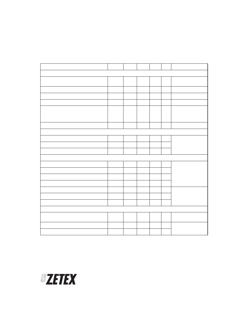
ZVP4525Z
S E M I C O N D U C T O R S
ISSUE 2 - JUNE 2007
ELECTRICAL CHARACTERISTICS (at T
amb
= 25°C unless otherwise stated)
PARAMETER
SYMBOL MIN.
TYP.
MAX.
UNIT CONDITIONS.
STATIC
Drain-Source Breakdown Voltage
V(BR)DSS -250
-285
V
ID=-1mA, VGS=0V
Zero Gate Voltage Drain Current
IDSS
-30
-500
nA
VDS=-250V, VGS=0V
Gate-Body Leakage
IGSS
±1
±100
nA
VGS=±40V, VDS=0V
Gate-Source Threshold Voltage
VGS(th) -0.8
-1.5
-2.0
V
I
D
=-1mA, VDS= VGS
Static Drain-Source On-State Resistance (1)
RDS(on)
10
13
14
18
Ω
Ω
VGS=-10V,
ID=-200mA
VGS=-3.5V,
ID=-100mA
Forward Transconductance (3)
gfs
80
200
mS
VDS=-10V,ID=-0.15A
DYNAMIC (3)
Input Capacitance
Ciss
73
pF
VDS=-25 V, VGS=0V,
f=1MHz
Output Capacitance
Coss
12.8
pF
Reverse Transfer Capacitance
Crss
3.91
pF
SWITCHING(2) (3)
Turn-On Delay Time
td(on)
1.53
ns
VDD =-30V, ID=-200m
A
RG=50Ω, VGS=-10V
(refer to test circuit)
Rise Time
tr
3.78
ns
Turn-Off Delay Time
td(off)
17.5
ns
Fall Time
tf
7.85
ns
Total Gate Charge
Qg
2.45
3.45
nC
VDS=-25V,VGS=-10V,
I
D
=-200mA(refer to
test circuit)
Gate-Source Charge
Qgs
0.22
0.31
nC
Gate Drain Charge
Qgd
0.45
0.63
nC
SOURCE-DRAIN DIODE
Diode Forward Voltage (1)
VSD
0.97
V
Tj=25°C, IS=-200mA,
VGS=0V
Reverse Recovery Time (3)
trr
205
290
ns
Tj=25°C, IF=-200mA,
di/dt=100A/
μs
Reverse Recovery Charge (3)
Qrr
21
29
nC
(1) Measured under pulsed conditions. Width=300
μs. Duty cycle ≤ 2% .
(2) Switching characteristics are independent of operating junction temperature.
(3) For design aid only, not subject to production testing.