Zvp4525z, Thermal resistance, Absolute maximum ratings – Diodes ZVP4525Z User Manual
Page 2
ZVP4525Z
S E M I C O N D U C T O R S
ISSUE 2 - JUNE 2007
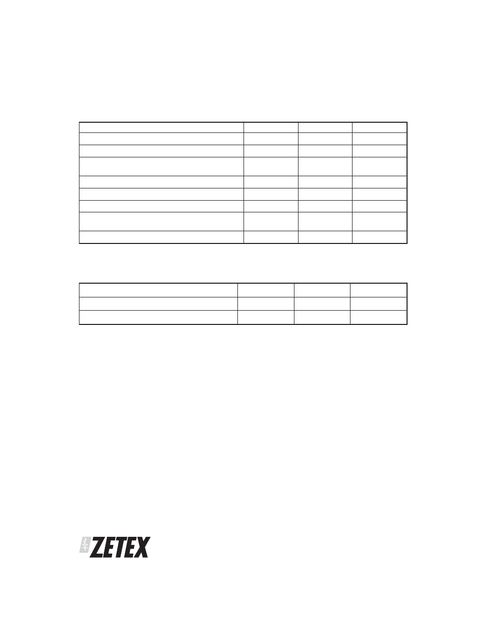
THERMAL RESISTANCE
PARAMETER
SYMBOL
VALUE
UNIT
Junction to Ambient (a)
RθJA
103
°C/W
Junction to Ambient (b)
RθJA
50
°C/W
NOTES
(a) For a device surface mounted on 25mm x 25mm FR4 PCB with high coverage of single sided 1oz copper, in still air conditions
(b) For a device surface mounted on FR4 PCB measured at t
р5 secs.
(c) Repetitive rating - pulse width limited by maximum junction temperature. Refer to Transient Thermal Impedance graph.
NB High Voltage Applications
For high voltage applications, the appropriate industry sector guidelines should be considered with regard to
voltage spacing between conductors.
ABSOLUTE MAXIMUM RATINGS
PARAMETER
SYMBOL
LIMIT
UNIT
Drain-Source Voltage
VDSS
250
V
Gate Source Voltage
VGS
±40
V
Continuous Drain Current (VGS=10V; TA=25°C)(a)
(VGS=10V; TA=70°C)(a)
ID
ID
-205
-164
mA
mA
Pulsed Drain Current (c)
IDM
-1
A
Continuous Source Current (Body Diode)
IS
-0.75
A
Pulsed Source Current (Body Diode)
ISM
-1
A
Power Dissipation at TA=25°C (a)
Linear Derating Factor
PD
1.2
9.6
W
mW/°C
Operating and Storage Temperature Range
Tj
:
Tstg
-55 to +150
°C
2