Absolute maximum ratings, Thermal resistance, Zxmp6a16k – Diodes ZXMP6A16K User Manual
Page 2
ZXMP6A16K
© Zetex Semiconductors plc 2007
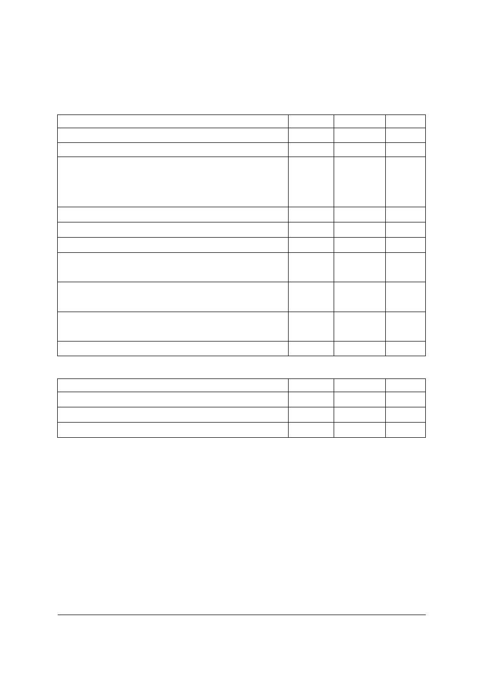
Absolute maximum ratings
NOTES:
(a) For a device surface mounted on 50mm x 50mm x 1.6mm FR4 PCB with high coverage of single sided 2oz copper, in
still air conditions.
(b) For a device surface mounted on FR4 PCB measured at t
Յ
10 sec.
(c) Repetitive rating 50mm x 50mm x 1.6mm FR4 PCB, D=0.02 pulse width=300
s - pulse width limited by maximum
junction temperature.
(d) For a device surface mounted on 25mm x 25mm x 1.6mm FR4 PCB with high coverage of single sided 1oz copper, in
still air conditions.
Parameter
Symbol
Limit
Unit
Drain-source voltage
V
DSS
-60
V
Gate-source voltage
V
GS
± 20
V
Continuous drain current
@ V
GS
= 10V; T
amb
=25°C
I
D
8.2
A
@ V
GS
= 10V; T
amb
=70°C
6.5
@ V
GS
= 10V; T
amb
=25°C
5.4
Pulsed drain current
I
DM
27.2
A
Continuous source current (body diode)
I
S
10
A
Pulsed source current (body diode)
I
SM
27.2
A
Power dissipation at T
amb
=25°C
P
D
4.24
W
Linear derating factor
33.9
mW/°C
Power dissipation at T
amb
=25°C
P
D
9.76
W
Linear derating factor
78
mW/°C
Power dissipation at T
amb
=25°C
P
D
2.11
W
Linear derating factor
16.8
mW/°C
Operating and storage temperature range
T
j
, T
stg
-55 to +150
°C
Thermal resistance
Parameter
Symbol
Limit
Unit
Junction to ambient
R
⍜JA
29.45
°C/W
Junction to ambient
R
⍜JA
12.8
°C/W
Junction to ambient
R
⍜JA
59.1
°C/W