Maximum ratings, Thermal characteristics – Diodes ZXMN10B08E6 User Manual
Page 2
ZXMN10B08E6
Datasheet Number: DS33570 Rev. 2 – 2
2 of 7
May 2014
© Diodes Incorporated
ZXMN10B08E6
NEW PROD
UC
T
Maximum Ratings
(@T
A
= +25°C, unless otherwise specified.)
Characteristic Symbol
Value
Unit
Drain-Source Voltage
V
DSS
100 V
Gate-Source Voltage
V
GS
±20
V
Continuous Drain Current
V
GS
= 10V
(Note 6)
I
D
1.9
A
T
A
= +70
°C (Note 6)
1.5
(Note 5)
1.6
Pulsed Drain Current
(Note 7)
I
DM
9 A
Continuous Source Current (Body Diode)
(Note
6)
I
S
2.5 A
Pulsed Source Current (Body Diode)
(Note
7)
I
SM
9 A
Thermal Characteristics
(@T
A
= +25°C, unless otherwise specified.)
Characteristic Symbol
Value
Unit
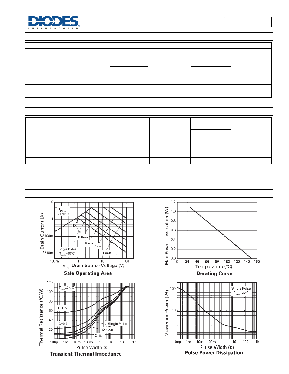
Power Dissipation (Note 5)
Linear Derating Factor
P
D
1.1
W
mW/
°C
8.8
Power Dissipation (Note 6)
Linear Derating Factor
P
D
1.7
W
mW/
°C
13.6
Thermal Resistance, Junction to Ambient
(Note 5)
R
θJA
113
°C/W
(Note 6)
73
Operating and Storage Temperature Range
T
J
, T
STG
-55 to +150
°C
Notes:
5. For a device surface mounted on 25mm x 25mm FR4 PCB with high coverage of single sided 1oz copper, in still air conditions
6. For a device surface mounted on FR4 PCB measured at t ≤ 5 secs.
7. Repetitive rating 25mm x 25mm FR4 PCB, D = 0.02, pulse width 300µs - pulse width limited by maximum junction temperature. Refer to Transient
Thermal Impedance graph.
Thermal Characteristics