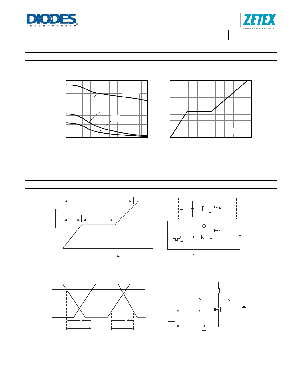
Typical characteristics, Test circuits, Capacitance v drain-source voltage – Diodes ZXMN10A25K User Manual
Page 6: Ccapacit ance (pf ) v, Drain - source voltage (v), Gate-source voltage v gate charge, Q - charge (nc), Zxmn10a25k, A product line of diodes incorporated, Ga te- s our ce vol tage ( v )
ZXMN10A25K
Document number: DS33569 Rev. 3 - 2
6 of 8
July 2012
© Diodes Incorporated
ZXMN10A25K
A Product Line of
Diodes Incorporated
Typical Characteristics
(cont.)
0.1
1
10
100
0
200
400
600
800
1000
1200
C
RSS
C
OSS
C
ISS
V
GS
= 0V
f = 1MHz
C
Capacit
ance (pF
)
V
DS
- Drain - Source Voltage (V)
0
2
4
6
8
10
12
14
16
18
0
2
4
6
8
10
I
D
= 2.9A
V
DS
= 50V
Gate-Source Voltage v Gate Charge
Capacitance v Drain-Source Voltage
Q - Charge (nC)
V
GS
G
a
te-
S
our
ce
Vol
tage (
V
)
Test Circuits
Current
regulator
Charge
Gate charge test circuit
Switching time test circuit
Basic gate charge waveform
Switching time waveforms
D.U.T
50k
0.2
F
12V
Same as
D.U.T
V
GS
V
GS
V
DS
V
G
Q
GS
Q
GD
Q
G
V
GS
90%
10%
t
(on)
t
(on)
t
d(on)
t
r
t
r
t
d(off)
V
DS
V
DD
R
D
R
G
Pulse width
Ͻ 1S
Duty factor 0.1%
V
DS
I
D
I
G