Zxmn3a06dn8, Absolute maximum ratings, Thermal resistance – Diodes ZXMN3A06DN8 User Manual
Page 2
ZXMN3A06DN8
ISSUE 2 - OCTOBER 2002
2
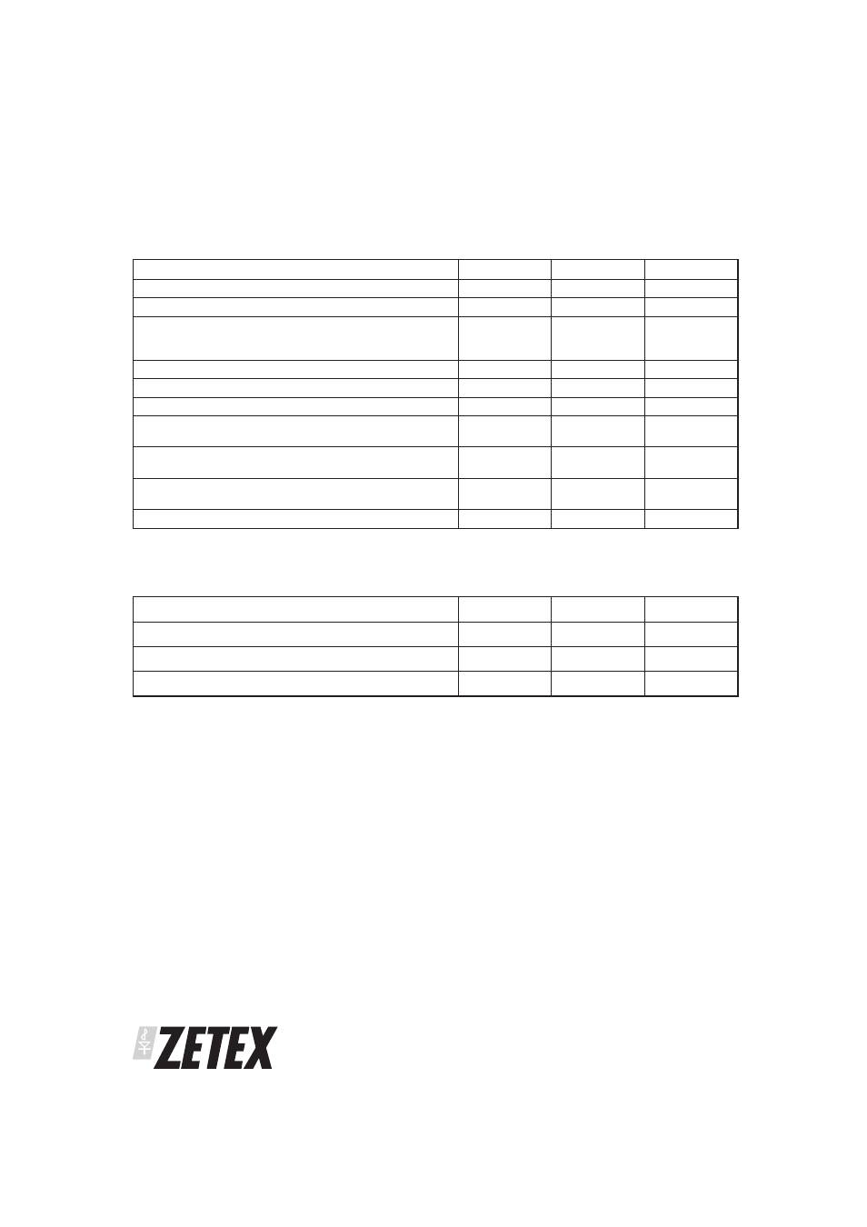
PARAMETER
SYMBOL
LIMIT
UNIT
Drain-Source Voltage
V
DSS
30
V
Gate Source Voltage
V
GS
Ϯ20
V
Continuous Drain Current (V
GS
=10V; T
A
=25°C)(b)(d)
(V
GS
=10V; T
A
=70°C)(b)(d)
(V
GS
=10V; T
A
=25°C)(a)(d)
I
D
6.2
5.0
4.9
A
Pulsed Drain Current (c)
I
DM
30
A
Continuous Source Current (Body Diode) (b)
I
S
3.7
A
Pulsed Source Current (Body Diode)(c)
I
SM
30
A
Power Dissipation at T
A
=25°C (a)(d)
Linear Derating Factor
P
D
1.25
10
W
mW/°C
Power Dissipation at T
A
=25°C (a)(e)
Linear Derating Factor
P
D
1.80
14.5
W
mW/°C
Power Dissipation at T
A
=25°C (b)(d)
Linear Derating Factor
P
D
2.1
17.3
W
mW/°C
Operating and Storage Temperature Range
T
j
:T
stg
-55 to +150
°C
ABSOLUTE MAXIMUM RATINGS.
PARAMETER
SYMBOL
VALUE
UNIT
Junction to Ambient (a)(d)
R
θ
JA
100
°C/W
Junction to Ambient (a)(e)
R
θ
JA
69
°C/W
Junction to Ambient (b)(d)
R
θ
JA
58
°C/W
NOTES
(a) For a device surface mounted on 25mm x 25mm FR4 PCB with high coverage of single sided 1oz copper, in still air conditions
(b) For a device surface mounted on FR4 PCB measured at t
р10 secs.
(c) Repetitive rating 25mm x 25mm FR4 PCB, D=0.02 pulse width=300µs - pulse width limited by maximum junction temperature. Refer to
Transient Thermal Impedance graph.
(d) For device with one active die
(e) For device with two active die running at equal power.
THERMAL RESISTANCE