Maximum ratings, Thermal characteristics, Zxmn3a01z – Diodes ZXMN3A01Z User Manual
Page 2
ZXMN3A01Z
Document number DS35722 Rev. 1 - 2
2 of 6
February 2012
© Diodes Incorporated
ZXMN3A01Z
ADVAN
CE I
N
F
O
RM
ATI
O
N
A Product Line of
Diodes Incorporated
Maximum Ratings
@T
A
= 25°C unless otherwise specified
Characteristic
Symbol
Value
Unit
Drain-Source Voltage
V
DSS
30 V
Gate-Source Voltage
V
GSS
±20 V
Continuous Drain Current
Steady
State
@ V
GS
= 10V ; T
A
= 25°C (Note 5)
@ V
GS
= 10V ;
T
A
= 75°C (Note 5)
@ V
GS
= 10V ; T
A
= 75°C (Note 4)
I
D
3.3
2.7
2.2
A
Pulsed Drain Current (Note 6)
I
DM
20 A
Continuous Source Current (Body Diode) (Note 5)
I
S
3.3 A
Pulsed Source Current (Body Diode) (Note 6)
I
SM
20 A
Thermal Characteristics
@T
A
= 25°C unless otherwise specified
Characteristic Symbol
Value
Unit
Power Dissipation
(Note 4)
P
D
0.97 W
(Note 5)
2.12
W
Thermal Resistance, Junction to Ambient
(Note 4)
R
θJA
129 °C/W
(Note 5)
59
°C/W
Operating and Storage Temperature Range
T
J
,
T
STG
-55 to +150
°C
Notes:
4. Device mounted on FR-4 substrate PC board, 2oz copper, with minimum recommended pad layout
5. Device mounted on 25mm X 25mm FR-4 substrate PC board with 2oz copper
6. Single pulse rating - 25mm x 25mm FR4 PCB, D=0.02, pulse width 300us – pulse width limited by maximum junction temperature.
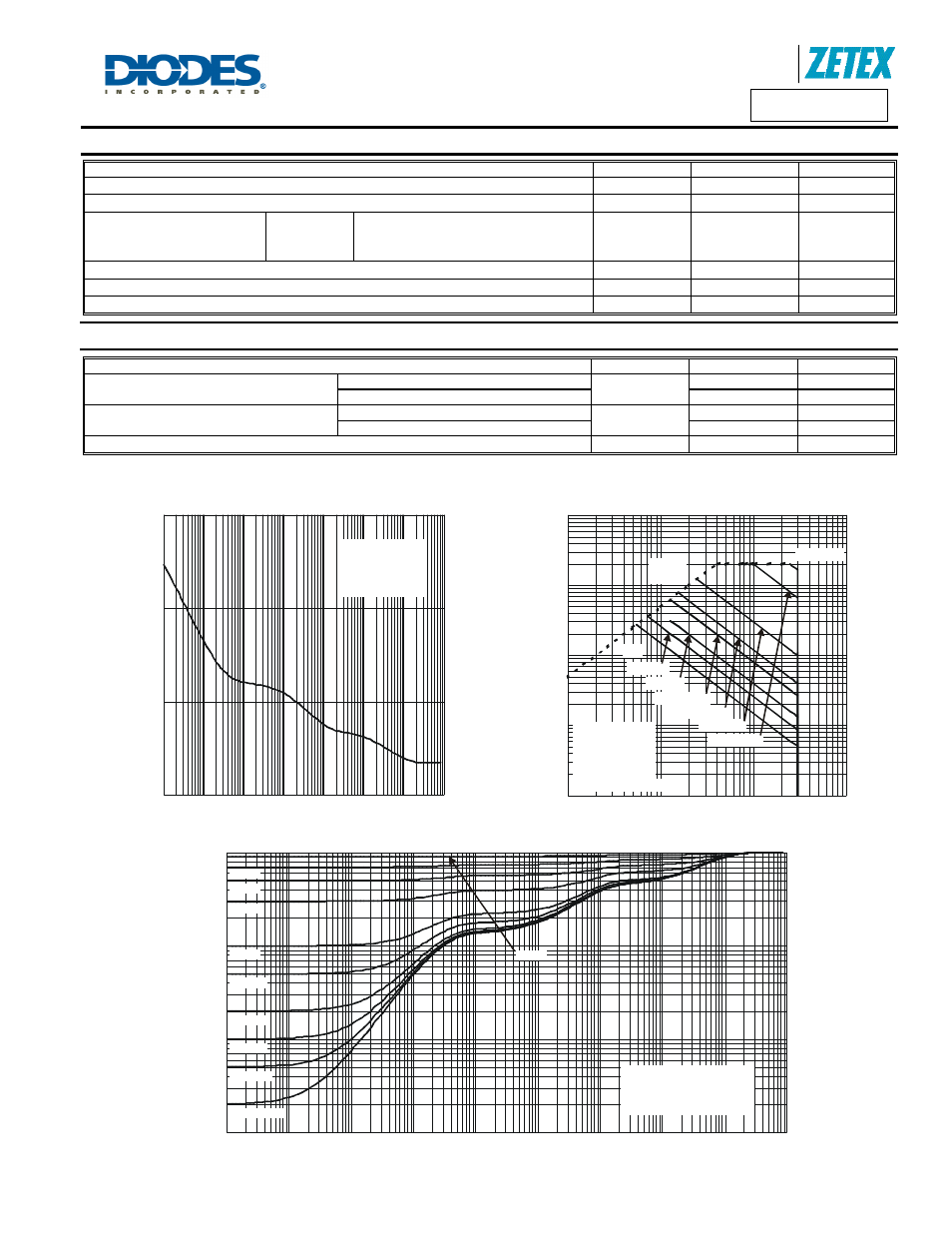
1
10
100
1,000
t1, PULSE DURATION TIME (sec)
Fig. 1 Single Pulse Maximum Power Dissipation
0.001 0.01
0.1
1
10
100
1,000
0.0001
P
,
P
E
AK
T
R
A
N
SI
E
N
T
P
O
IW
E
R
(W)
(PK)
Single Pulse
R
= 57 C/W
R
= r
* R
T - T = P * R
θ
θ
θ
θ
JA
JA(t)
(t)
JA
J
A
JA(t)
°
0.1
1
10
100
V
, DRAIN-SOURCE VOLTAGE (V)
Fig. 2 SOA, Safe Operation Area
DS
0.01
0.1
1
10
100
I,
D
R
AI
N
C
U
R
R
EN
T
(A
)
D
T
= 150°C
T = 25°C
J(max)
A
V
= 10V
Single Pulse
GS
DUT on 1in. Board
2
R
Limited
DS(on)
DC
P = 10s
W
P = 1s
W
P = 100ms
W
P = 10ms
W
P = 1ms
W
P = 100µs
W
P = 10 s
W
µ
0.00001
0.0001
0.001
0.01
0.1
1
10
100
1,000
t1, PULSE DURATION TIMES (sec)
Fig. 3 Transient Thermal Resistance
0.00001
0.001
0.01
0.1
r(t),
T
R
AN
S
IEN
T
T
H
E
R
MA
L
R
ES
IS
T
AN
C
E
1
R
(t) = r(t) * R
R
= 57°C/W
Duty Cycle, D = t1/ t2
θ
θ
θ
JA
JA
JA
D = 0.7
D = 0.9
D = 0.5
D = 0.3
D = 0.1
D = 0.05
D = 0.02
D = 0.01
D = 0.005
Single Pulse