Diodes ZXMN2088DE6 User Manual
Page 2
ZXMN2088DE6
Ab
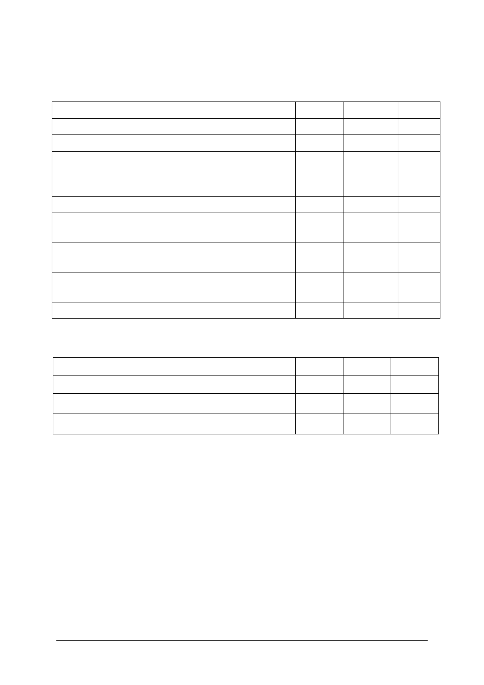
solute maximum ratings
Parameter Symbol
Limit
Unit
Drain-Source voltage
V
DSS
20 V
Gate-Source voltage
V
GS
± 8
V
Continuous Drain current @ V
GS
= 4.5V; T
A
=25
°C
(b) (d)
@ V
GS
= 4.5V; T
A
=70
°C
(b) (d)
@ V
GS
= 4.5V; T
A
=25
°C
(a) (d)
I
D
2.1
1.7
1.7
A
Pulsed Drain current
(c)
I
DM
8 A
Power dissipation at T
A
=25
°C
(a) (d)
Linear derating factor
P
D
0.9
7.2
W
mW/
°C
Power dissipation at T
A
=25
°C
(a) (e)
Linear derating factor
P
D
1.1
8.8
W
mW/
°C
Power dissipation at T
A
=25
°C
(b) (d)
Linear derating factor
P
D
1.3
10.4
W
mW/
°C
Operating and storage temperature range
T
j
, T
stg
-55 to +150
°C
Thermal resistance
Parameter Symbol
Value
Unit
Junction to Ambient
(a) (d)
R
θJA
139
°C/W
Junction to Ambient
(a)
(e)
R
θJA
113
°C/W
Junction to Ambient
(b)
(d)
R
θJA
96
°C/W
NOTES:
(a) For a device surface mounted on 25mm x 25mm FR4 PCB with high coverage of single sided 1oz copper, in
still air conditions.
(b) As above measured at t
≤ 5 sec.
(c) Repetitive rating - 25mm x 25mm FR4 PCB, D=0.02, pulse width 300us – pulse width limited by maximum
junction temperature.
(d) For device with one active die
(e) For device with two active die running at equal power.
Issue 2 – June 2008
2
www.zetex.com
© Diodes Incorporated 2008
www.diodes.com