Absolute maximum ratings, Thermal resistance, Esd rating – Diodes ZXGD3102 User Manual
Page 2
Issue 4, May 2009
2
©Diodes Incorporated 2008
ZXGD3102T8
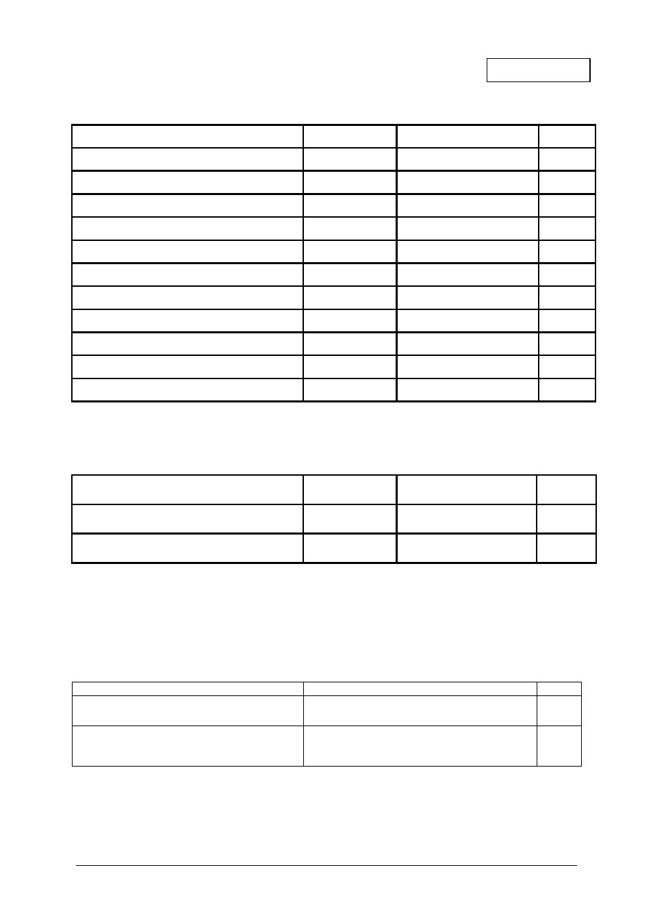
Absolute maximum ratings
Parameter Symbol
Limit
Unit
Supply voltage
1
V
CC
15
V
Continuous Drain pin voltage
1
V
D
-3
to180
V
GATEH and GATEL output Voltage
1
V
G
-3 to V
CC
+ 3
V
Driver peak source current
I
SOURCE
4
A
Driver peak sink current
I
SINK
7
A
Reference current
I
REF
25
mA
Bias voltage
V
BIAS
V
CC
V
Bias current
I
BIAS
100
mA
Power dissipation at T
A
=25
°C
P
D
500
mW
Operating junction temperature
T
j
-40 to +150
°C
Storage temperature
T
stg
-50 to +150
°C
Notes:
1. All voltages are relative to GND pin
Thermal resistance
Parameter Symbol
Value
Unit
Junction to ambient (*)
R
θJA
250
°C/W
Junction to case (†)
R
θJC
54
°C/W
Notes:
(*) Mounted on minimum 1oz copper on FR4 PCB in still air conditions
(†) Junction to solder point at the end of the lead 5 and 6
ESD Rating
Model Rating
Unit
Human body
4,000
V
Machine 400
V