Electrical characteristics, A product line of diodes incorporated – Diodes ZXGD3104N8 User Manual
Page 5
ZXGD3104N8
Document Number DS35546
Rev. 1 – 2
5 of 13
November 2011
© Diodes Incorporated
A Product Line of
Diodes Incorporated
ZXGD3104N8
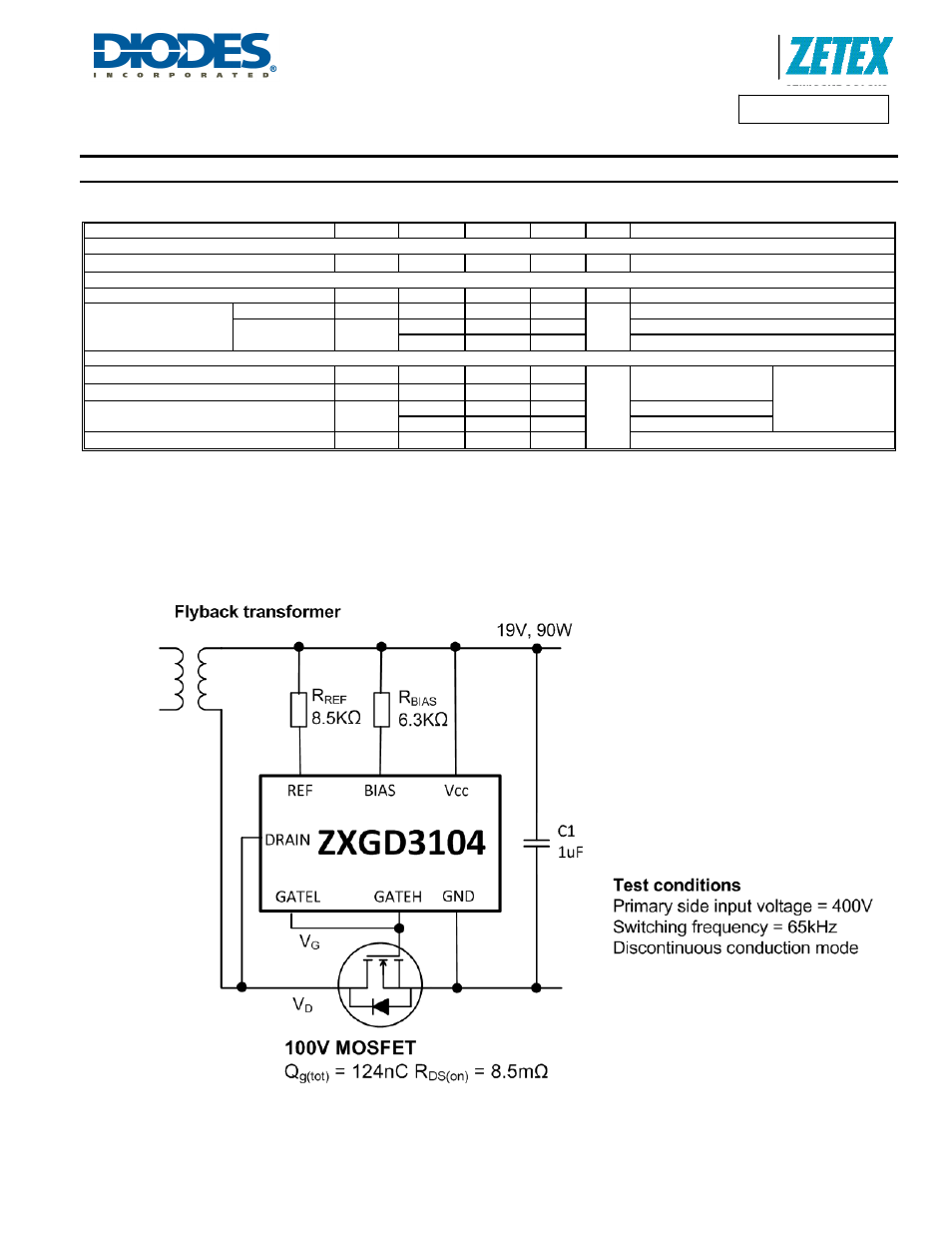
Electrical Characteristics
@T
A
= 25°C unless otherwise specified
V
CC
= 19V; R
BIAS
= 6.3k
Ω; R
REF
= 8.5k
Ω
Characteristic Symbol
Min
Typ
Max
Unit Test
Condition
Input and Supply
Quiescent current
I
Q
-
5.16
-
mA
V
D
≥ 0V
Gate Driver
Turn-off Threshold Voltage (Note 9 & 10)
V
T
-16 -10 0
mV
V
G
= 1V
Gate output voltage
(Note 9 & 10)
V
G(off)
0 0.73
1.0
V
V
D
≥ 1V
(Note 9 & 11)
V
G
12.5 14
V
CC
V
D
= -50mV
17 18
V
CC
V
D
= -100mV
Switching Performance for Q
G
(tot) = 124nC (Note 12)
Turn-on propagation delay
t
d(rise)
175 250 325
ns
-
Refer to switching
waveforms in Fig. 1
Turn-off propagation delay
t
d(fall)
11 15 20
Gate rise time
t
r
335
480
625
From 10% of V
G
to 10V
530
760
990
From 10% to 90% of V
G
Gate fall time
t
f
35
50
65
Continuous Conduction Mode
Notes:
9.GATEH connected to GATEL
10.R
H
= 100k
Ω, R
L
= O/C
11.R
L
= 100k
Ω, R
H
= O/C
12. refer to test circuit below