Maximum ratings, Thermal characteristics – Diodes ZXGD3104N8 User Manual
Page 3
ZXGD3104N8
Document Number DS35546
Rev. 1 – 2
3 of 13
November 2011
© Diodes Incorporated
A Product Line of
Diodes Incorporated
ZXGD3104N8
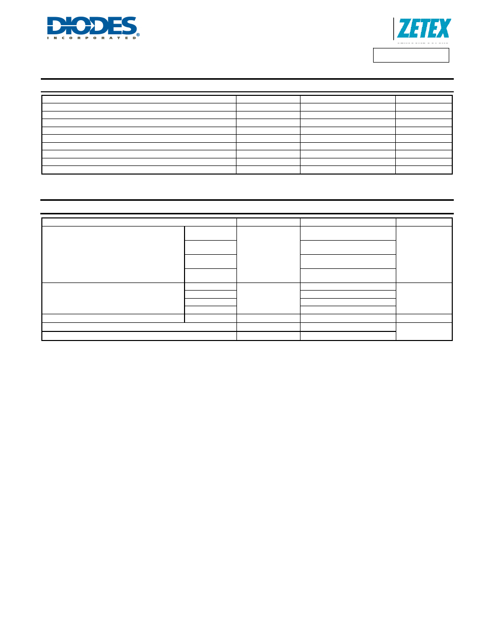
Maximum Ratings
@T
A
= 25°C unless otherwise specified
Characteristic Symbol
Value
Unit
Supply voltage, relative to GND
V
CC
25 V
Drain pin voltage
V
D
-3 to 180
V
Gate output voltage
V
G
-3 to V
CC
+ 3
V
Gate Driver peak source current
I
SOURCE
2.5 A
Gate Driver peak sink current
I
SINK
7 A
Reference voltage
V
REF
V
CC
V
Reference current
I
REF
25
mA
Bias voltage
V
BIAS
V
CC
V
Bias current
I
BIAS
100
mA
Thermal Characteristics
@T
A
= 25°C unless otherwise specified
Characteristic Symbol
Value
Unit
Power Dissipation
Linear derating factor
(Note 4)
P
D
490
3.92
mW
mW/
°C
(Note 5)
655
5.24
(Note 6)
720
5.76
(Note 7)
785
6.28
Thermal Resistance, Junction to Ambient
(Note 4)
R
θJA
255
°C/W
(Note 5)
191
(Note 6)
173
(Note 7)
159
Thermal Resistance, Junction to Lead
(Note 8)
R
θJL
135
°C/W
Operating Temperature Range
T
J
-40 to +150
°C
Storage Temperature Range
T
STG
-50 to +150
Notes:
4. For a device surface mounted on minimum recommended pad layout FR4 PCB with high coverage of single sided 1oz copper, in still air conditions; the
device is measured when operating in a steady-state condition.
5. Same as note (4), except pin 5 (V
CC
) and pin 6 (GND) are both connected to separate 5mm x 5mm 1oz copper heatsinks.
6. Same as note (5), except both heatsinks are 10mm x 10mm.
7. Same as note (5), except both heatsinks are 15mm x 15mm.
8. Thermal resistance from junction to solder-point at the end of each lead on pin 5 (V
CC
) and pin 6 (GND).