Diodes ZXGD3104N8 User Manual
Page 11

ZXGD3104N8
Document Number DS35546
Rev. 1 – 2
11 of 13
November 2011
© Diodes Incorporated
A Product Line of
Diodes Incorporated
ZXGD3104N8
Design considerations
It is advisable to decouple the ZXGD3104 closely to V
CC
and ground due to the possibility of high peak gate currents
with a 1
μF X7R type ceramic capacitor C1 as shown in Figure 2. Also the ground return loop should be as short as
possible.
To minimize parasitic inductance-induced premature turn-off of the synchronous controller always keep the PCB
track length between ZXGD3104’s Drain input and MOSFET’s Drain to less than 10mm. Low internal inductance
SMD MOSFET packages are also recommended for high switching frequency power conversion to minimize
MOSFET body diode conduction loss.
The Gate pins should be as close to the MOSFET’s gate as possible. External gate resistors are optional. They can
be inserted to control the rise and fall time which may help with EMI issues.
The careful selection of external resistors R
REF
and R
BIAS
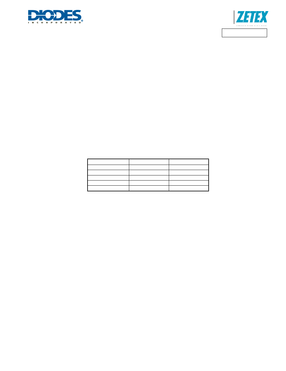
is important to the optimum device operation. Select a value
for resistor R
REF
and R
BIAS
from Table 1 based on the desired Vcc value. This provides the typical ZXGD3104’s
detection threshold voltage of -10mV.
Table 1. Recommended resistor values for various supply voltages
V
CC
R
BIAS
R
REF
5V
1.6
k
Ω
2
k
Ω
10V
3.3
k
Ω
4.3
k
Ω
12V
3.9
k
Ω
5.1
k
Ω
15V
5.1
k
Ω
6.8
k
Ω
19V
6.3
k
Ω
8.5
k
Ω
