Zhb6790, Safe operating area, Safe operating area (full copper) – Diodes ZHB6790 User Manual
Page 7: Safe operating area (minimum copper)
ZHB6790
100m
100
1s
100ms
10
DC
10m
V
CE
- Collector Emitter Voltage (V)
Safe Operating Area (Full Copper)
10ms
1ms
100µs
1
10
100m
1
100m
100
1s
100ms
10
DC
10m
VCE - Collector Emitter Voltage (V)
Safe Operating Area (Minimum Copper)
10ms
1ms
100µs
1
10
100m
1
see note below
see note below
ZETEX H Bridge NPN transistors Spice model Last revision 4/7/97
.MODEL H6790N NPN IS =2.505E-12 NF =1.0058 BF =1360 IKF=1.3 VAF=35
+ISE=.24E-12 NE =1.38 NR =1.001 BR =125 IKR=1 VAR=8 ISC=.435E-12
+NC =1.213 RB =.2 RE =.043 RC =.04 CJC=54.3E-12 MJC=.475 VJC=.765
+CJE=247E-12 TF =.851E-9 TR =15.7E-9
*
*
*ZETEX H Bridge PNP transistors Spice model Last revision 4/7/97
.MODEL H6790P PNP IS=1.09684E-12 NF=1.0102 BF=650 IKF=1.7 VAF=23.5
+ISE=9.88593E-14 NE=1.47256 NR=1.00391 BR=270 IKR=0.2 VAR=30
+ISC=5.4933E-14 NC=1.07427 RB=0.055 RE=0.049 RC=0.078 CJC=96E-12
+MJC=0.495 VJC=0.67 CJE=275E-12 TF=0.75E-9 TR=10.8E-9
*
(C) 1997 ZETEX PLC
The copyright in these models and the design embodied belong to Zetex PLC (Zetex). They are supplied
free of charge by Zetex for the purpose of research and design and may be used or copied intact (including
this notice) for that purpose only. All other rights are reserved. The models are believed accurate but no
condition or warranty as to their merchantability or fitness for purpose is given and no liability in respect of
any use is accepted by Zetex PLC, its distributors or agents. Zetex PLC, Fields New Road, Chadderton,
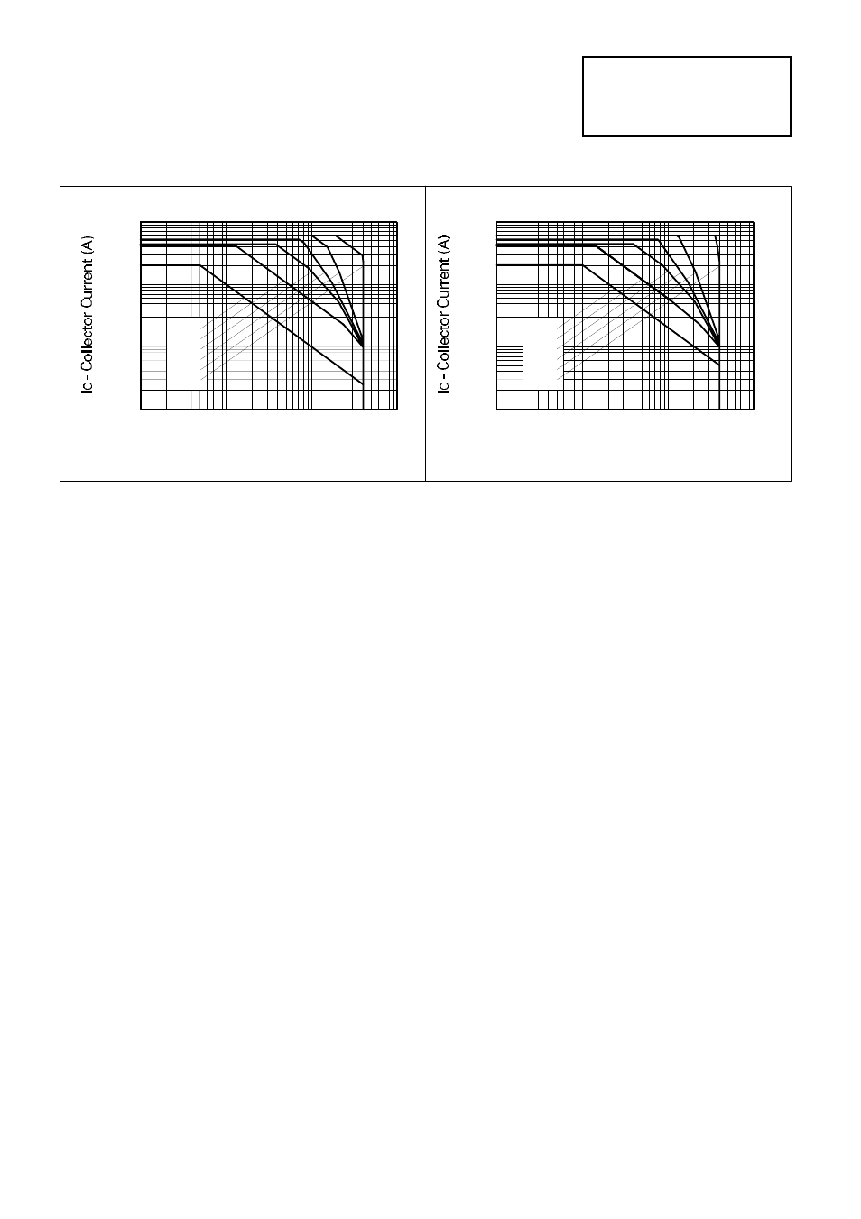
SAFE OPERATING AREA
Note: The Safe Operating Area (SOA) charts shown are a combination of the worst case secondary
breakdown characteristics for the NPN/PNP pair, and the thermal curves demonstrating the
power dissipation capability of the energised ZHB part (opposing NPN-PNP switched on) when
mounted on a 50mm x 50mm FR4 PCB. The two cases show:
i) full copper present and
ii) with minimal copper present - this being defined as an SM-8 footprint with 1.5mm tracks to
the edge of the PCB.
For example, on a 50mm x 50mm full copper PCB, the ZHB6790 will safely dissipate 2W under
DC conditions, taking note of continuous current ratings and voltage limits. Higher powers can
be tolerated for pulsed operation, while the shorter pulse widths (100
µ
s and 1ms) being relevant
for assessment of switching conditions.
The ZHB6790 H-Bridge can be modelled within SPICE using the following transistor models
configured in the standard H-Bridge topology, as shown in the schematic diagram of this datasheet.