Typical switching characteristics, Switching speed, Supply current – Diodes ZXGD3005E6 User Manual
Page 4: Asymmetric source and sink resistors, Vo lt ag e (v ) time (ns), Su p p ly curre nt (a ) frequency (hz), High load capacitance cl = 100nf time, S) v o lt ag e (v )
ZXGD3005E6
Document Number DS35095
Rev. 4 – 2
4 of 8
March 2011
© Diodes Incorporated
A Product Line of
Diodes Incorporated
ZXGD3005E6
ADVAN
CE I
N
F
O
RM
ATI
O
N
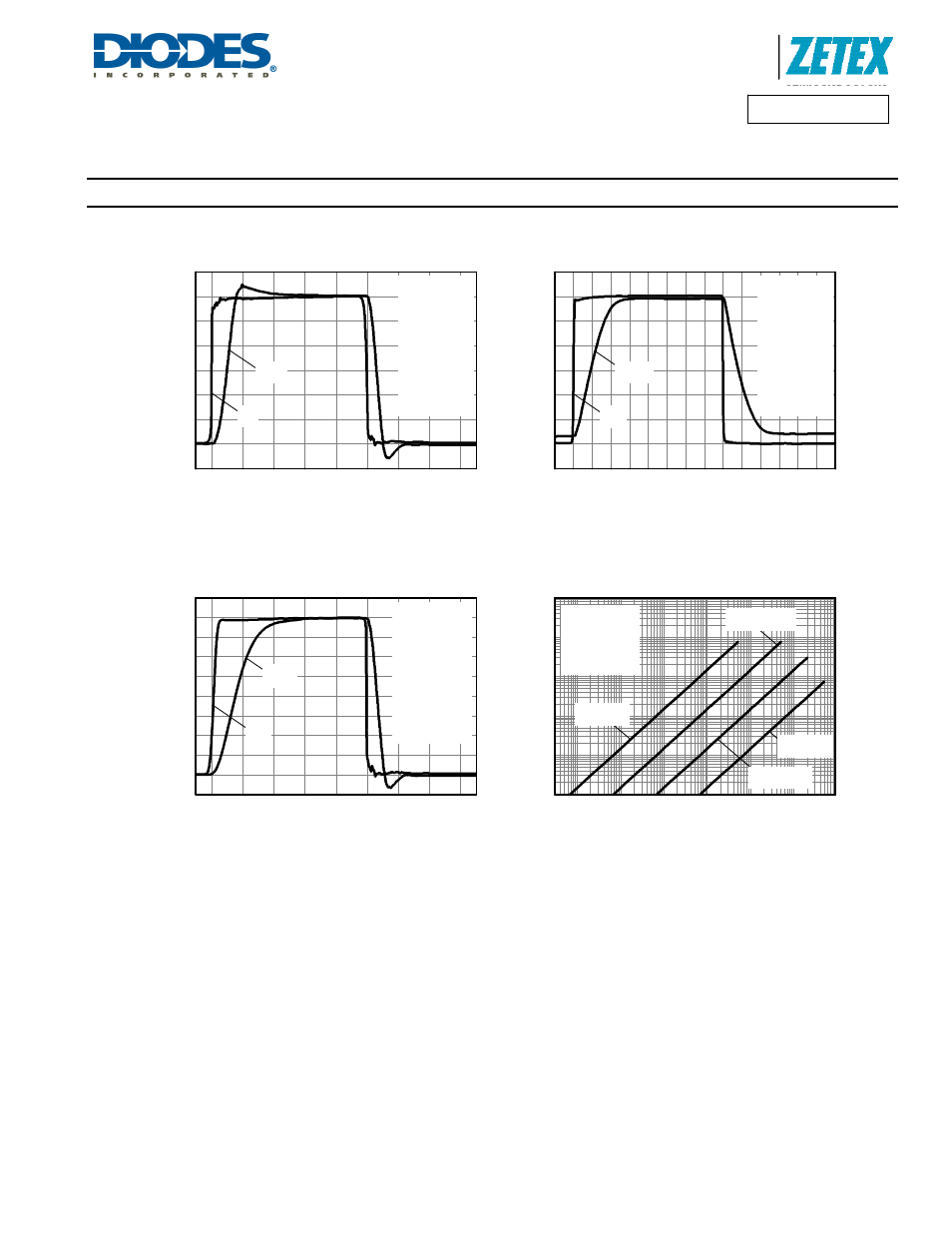
Typical Switching Characteristics
@T
A
= 25°C unless otherwise specified
0
100 200 300 400 500 600 700 800
-5
0
5
10
15
10
100
1k
10k
100k
1M
1E-4
1E-3
0.01
0.1
1
10
0
100 200 300 400 500 600 700 800
0
5
10
15
0.0
0.5
1.0
1.5
2.0
2.5
3.0
3.5
0
5
10
15
V
IN
= -5 to 15V
V
CC
= 15V
V
EE
= -5V
R
IN
= 1k
Ω
C
L
= 10nF
R
L
= 0.18
Ω
R
SOURCE
= 4.7
Ω
R
SINK
= 0
Ω
Switching Speed
Asymmetric Source and Sink Resistors
V
IN
V
OUT
V
o
lt
ag
e (V
)
Time (ns)
V
IN
= 0 to 15V
V
CC
= 15V
V
EE
= 0V
Square W ave
C
L
= 1
μ
F
C
L
= 100nF
C
L
= 10nF
Supply Current
S
u
p
p
ly
Curre
nt
(A
)
Frequency (Hz)
C
L
= 1nF
V
IN
= 0 to 15V
V
CC
= 15V
V
EE
= 0V
R
IN
= 1k
Ω
C
L
= 10nF
R
L
= 0.18
Ω
R
SOURCE
= 0
Ω
R
SINK
= 0
Ω
V
OUT
Switching Speed
Low Load Capacitance CL = 10nF
V
o
lt
a
ge (V
)
Time (ns)
V
IN
V
IN
= 0 to 15V
V
CC
= 15V
V
EE
= 0V
R
IN
= 1k
Ω
C
L
= 100nF
R
L
= 0.18
Ω
R
SOURCE
= 0
Ω
R
SINK
= 0
Ω
V
OUT
V
IN
Switching Speed
High Load Capacitance CL = 100nF
Time (
μ
s)
V
o
lt
ag
e (V
)