Typical application circuit, Maximum ratings, Thermal characteristics – Diodes ZXGD3005E6 User Manual
Page 2
ZXGD3005E6
Document Number DS35095
Rev. 4 – 2
2 of 8
March 2011
© Diodes Incorporated
A Product Line of
Diodes Incorporated
ZXGD3005E6
ADVAN
CE I
N
F
O
RM
ATI
O
N
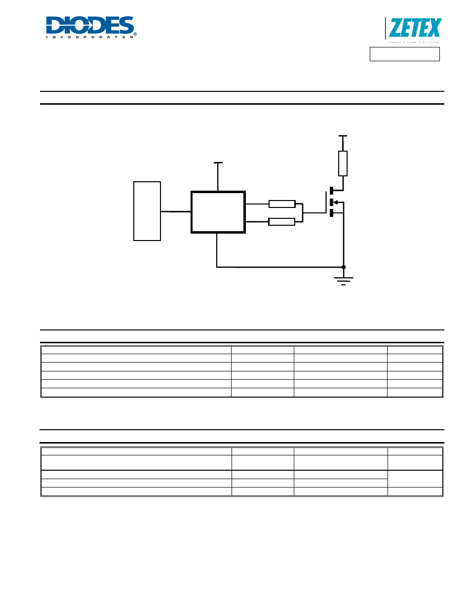
Typical Application Circuit
Maximum Ratings
@T
A
= 25°C unless otherwise specified
Characteristic Symbol
Value
Unit
Supply voltage, with respect to V
EE
V
CC
25 V
Input voltage, with respect to V
EE
V
IN
25 V
Output difference voltage (Source – Sink)
ΔV
(source-sink)
±7.5 V
Peak output current
I
PK
±10 A
Input current
I
IN
±100 mA
Thermal Characteristics
@T
A
= 25°C unless otherwise specified
Characteristic Symbol
Value
Unit
Power Dissipation (Notes 4 & 5)
Linear derating factor
P
D
1.1
8.8
W
mW/
°C
Thermal Resistance, Junction to Ambient (Notes 4 & 5)
R
θJA
113
°C/W
Thermal Resistance, Junction to Lead (Note 6)
R
θJL
105
Operating and Storage Temperature Range
T
J,
T
STG
-55 to +150
°C
Notes:
4. For a device surface mounted on 25mm x 25mm x 0.6mm FR4 PCB with high coverage of single sided 1oz copper, in still air conditions; the device is
measured when operating in a steady-state condition. The heatsink is split in half with the pin 1 (V
CC
) and pin 3 (V
EE
) connected separately to each half.
5. For device with two active die running at equal power.
6. Thermal resistance from junction to solder-point at the end of each lead on pin 1 (V
CC
) and pin 3 (V
EE
).
IN
V
CC
ZXGD3005
V
S
V
CC
V
EE
SOURCE
SINK
R
SOURCE
R
SINK
Controlle
r IC