Maximum ratings, Thermal characteristics – Diodes ZXTN26070CV User Manual
Page 2
ZXTN26070CV
Document number: DS32129 Rev. 3 - 2
2 of 7
April 2010
© Diodes Incorporated
A Product Line of
Diodes Incorporated
ZXTN26070CV
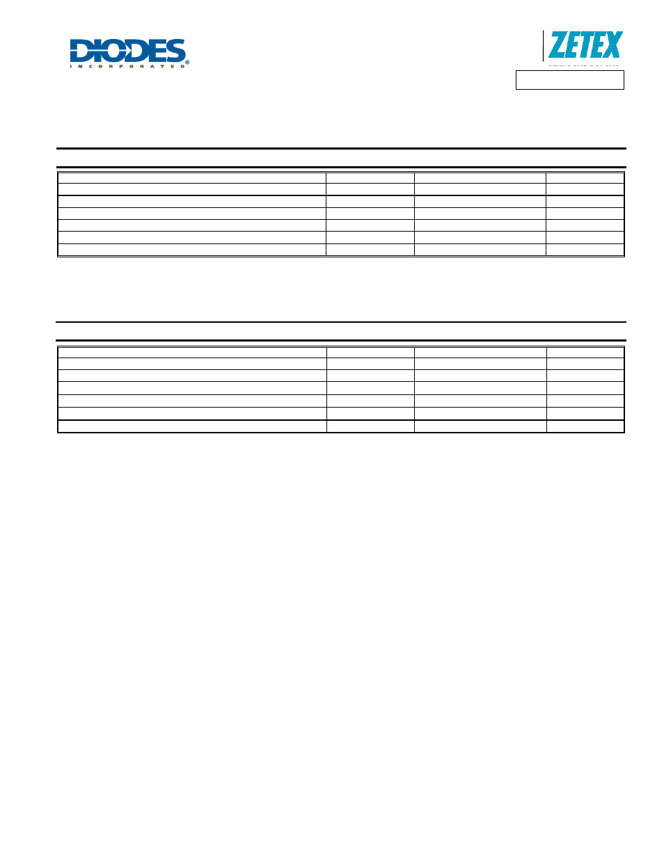
Maximum Ratings
@T
A
= 25°C unless otherwise specified
Characteristic Symbol
Value
Unit
Collector-Base Voltage
V
CBO
150 V
Collector-Emitter Voltage
V
CEO
70 V
Emitter-Base Voltage
V
EBO
7 V
Continuous Collector Current
I
C
2 A
Peak Pulse Current
I
CM
5 A
Base Current
I
B
500 A
Thermal Characteristics
Characteristic Symbol
Value
Unit
Power Dissipation at T
A
= 25
°C (Note 4)
P
D
0.6 W
Power Dissipation at T
A
= 25
°C (Note 5)
P
D
1 W
Thermal Resistance, Junction to Ambient (Note 4) @ T
A
= 25
°C
R
θJA
208
°C/W
Thermal Resistance, Junction to Ambient (Note 5) @ T
A
= 25
°C
R
θJA
121
°C/W
Thermal Resistance, Junction to Lead (Note 6)
R
θJL
37
°C/W
Operating and Storage Temperature Range
T
J,
T
STG
-55 to +150
°C
Notes:
4. For a device surface mounted minimum recommended pad layout, in still air conditions
5. Mounted on 25mm X 25mm X 1.6mm FR4 PCB with high coverage of single sided 2 oz copper, in still air conditions.
6. From Collector leads. Typical.