Zxtn2031f, Absolute maximum ratings thermal resistance – Diodes ZXTN2031F User Manual
Page 2
ZXTN2031F
© Zetex Semiconductors plc 2006
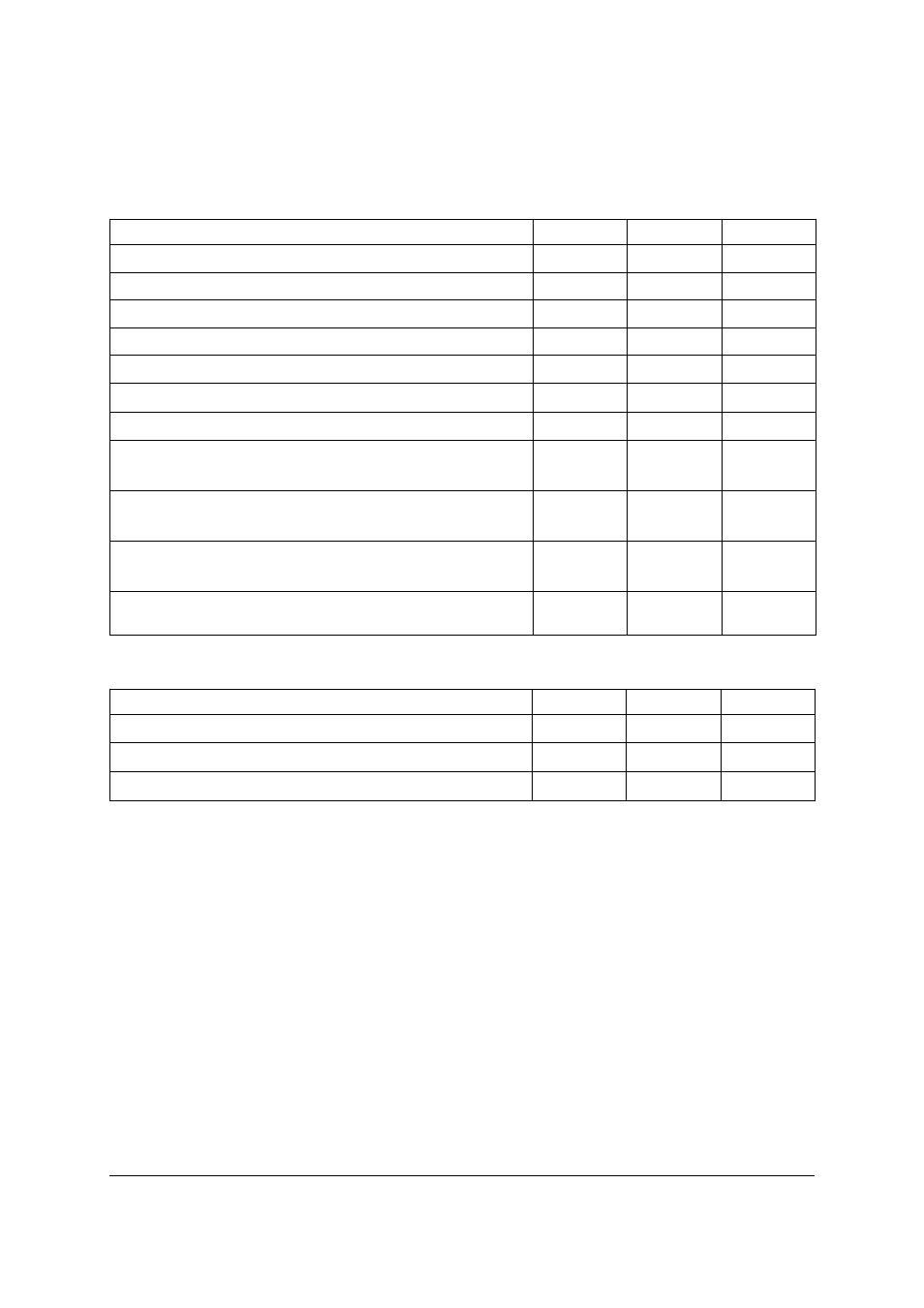
Absolute maximum ratings
Thermal resistance
Parameter
Symbol
Limit
Unit
Collector-base voltage
V
CBO
80
V
Collector-emitter voltage
V
(BR)CEV
80
V
Collector-emitter voltage
V
CEO
50
V
Emitter-base voltage
V
EBO
7.0
V
Peak pulse current
I
CM
12
A
Continuous collector current
I
C
5
A
Base current
I
B
1.2
A
Power dissipation @ T
A
=25
o
C
Linear derating factor
P
D
1.0
8.0
W
mW/
o
C
Power dissipation @ T
A
=25
o
C
Linear derating factor
P
D
1.2
9.6
W
mW/
o
C
Power dissipation @ T
A
=25
o
C
Linear derating factor
P
D
1.56
12.5
W
mW/
o
C
Operating and storage temperature
T
j
:T
stg
-55 to
+150
o
C
Parameter
Symbol
Value
Unit
Junction to ambient
(a)
NOTES:
(a) Mounted on 18mm x 18mm x 1.6mm FR4 PCB with a very high coverage of 2 oz weight copper in still air conditions.
Rθ
JA
125
o
C/W
Junction to ambient
(b)
(b) Mounted on 30mm x 30mm x 1.6mm FR4 PCB with a very high coverage of 2 oz weight copper in still air conditions.
Rθ
JA
104
o
C/W
Junction to ambient
(c)
(c) As (b) above measured at t<5secs.
Rθ
JA
80
o
C/W