Zxt849k – Diodes ZXT849K User Manual
Page 2
ZXT849K
S E M I C O N D U C T O R S
ISSUE 2 - DECEMBER 2003
2
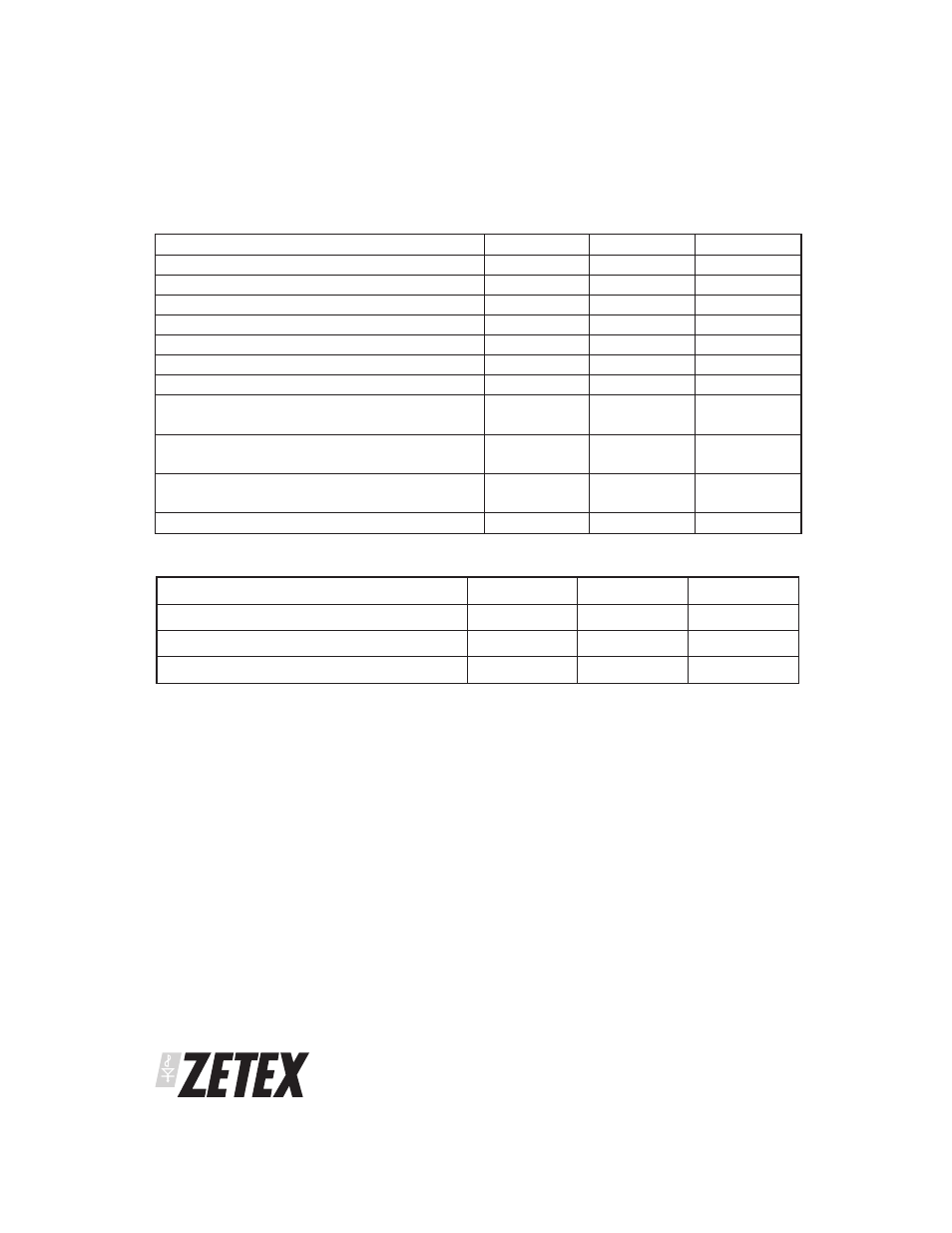
PARAMETER
SYMBOL
VALUE
UNIT
Junction to ambient
(a)
R
⍜JA
59
°C/W
Junction to ambient
(b)
R
⍜JA
39
°C/W
Junction to ambient
(c)
R
⍜JA
30
°C/W
NOTES
(a) (For a device surface mounted on 25mm x 25mm x 1.6mm FR4 PCB with high coverage of single sided 1oz copper in still air conditions.
(b) For a device surface mounted on 50mm x 50mm x 1.6mm FR4 PCB with high coverage of single sided 1oz copper in still air conditions.
(c) For a device surface mounted on 25mm x 25mm x 1.6mm FR4 PCB with high coverage of single sided 2oz copper in still air conditions.
THERMAL RESISTANCE
PARAMETER
SYMBOL
LIMIT
UNIT
Collector-base voltage
BV
CBO
80
V
Collector-emitter voltage
BV
CER
80
V
Collector-emitter voltage
BV
CEO
30
V
Emitter-base voltage
BV
EBO
7
V
Peak pulse current
I
CM
20
A
Continuous collector current
(b)
I
C
7
A
Base current
I
B
0.5
A
Power dissipation at T
A
=25°C
(a)
Linear derating factor
P
D
2.1
16.8
W
mW/°C
Power dissipation at T
A
=25°C
(b)
Linear derating factor
P
D
3.2
25.6
W
mW/°C
Power dissipation at T
A
=25°C
(c)
Linear derating factor
P
D
4.2
33.6
W
mW/°C
Operating and storage temperature range
T
j
, T
stg
-55 to +150
°C
ABSOLUTE MAXIMUM RATINGS