Electrical characteristics – q1 (npn transistor) – Diodes ZXTC2061E6 User Manual
Page 4
ZXTC2061E6
Document Number: DS33646 Rev: 2 - 2
4 of 9
February 2013
© Diodes Incorporated
ZXTC2061E6
ADVAN
CE I
N
F
O
RM
ATI
O
N
A Product Line of
Diodes Incorporated
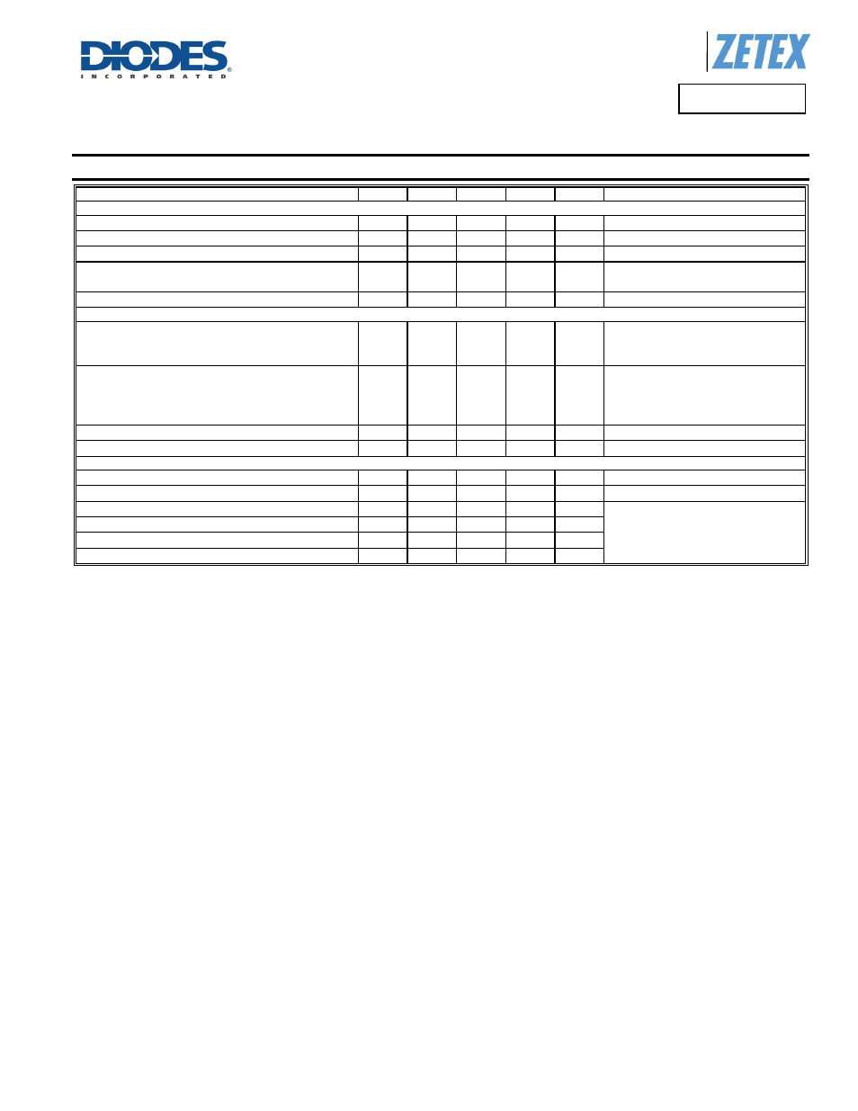
Electrical Characteristics – Q1 (NPN Transistor)
(@T
A
= +25°C, unless otherwise specified.)
Characteristic Symbol
Min
Typ
Max
Unit
Test
Condition
OFF CHARACTERISTICS
Collector-Base Breakdown Voltage
BV
CBO
20 40 — V
I
C
= 100µA, I
E
= 0
Collector-Emitter Breakdown Voltage (Note 12)
BV
CEO
12 17 — V
I
C
= 10mA, I
B
= 0
Emitter-Base Breakdown Voltage
BV
EBO
7 8.4 — V
I
E
= 100µA, I
C
= 0
Collector Cutoff Current
I
CBO
—
<1
50
0.5
nA
µA
V
CB
= 20V
V
CB
= 20V, T
A
= +100°C
Collector Cutoff Current
I
EBO
— <1 50 nA
V
EB
= 5.6V
ON CHARACTERISTICS (Note 12)
DC Current Gain
h
FE
500
480
260
800
750
390
1500
—
I
C
= 10mA, V
CE
= 2V
I
C
= 1.0A, V
CE
= 2V
I
C
= 5A, V
CE
= 2V
Collector-Emitter Saturation Voltage
V
CE(sat)
—
32
50
65
145
40
60
80
180
mV
I
C
= 1.0A, I
B
= 100mA
I
C
= 1.0A, I
B
= 10mA
I
C
= 2.0A, I
B
= 40mA
I
C
= 5A, I
B
= 100mA
Base-Emitter Saturation Voltage
V
BE(sat)
— 920
1000 mV
I
C
= 5A, I
B
= 100mA
Base-Emitter Turn-On Voltage
V
BE(on)
— 810 900 mV
I
C
= 5A, V
CE
= 2V
SMALL SIGNAL CHARACTERISTICS
Output Capacitance
C
obo
— 26 35 pF
V
CB
= 10V, f = 1.0MHz
Current Gain-Bandwidth Product
f
T
— 260 — MHz
V
CE
= 10V, I
C
= 50mA, f = 100MHz
Delay Time
t
d
— 71 — ns
V
CC
= 10V, I
C
= 1A, I
B1
= -I
B2
= 10mA
Rise Time
t
r
— 70 — ns
Storage Time
t
s
— 233 — ns
Fall Time
t
f
— 72 — ns
Notes:
12. Measured under pulsed conditions. Pulse width
≤ 300μs. Duty cycle ≤ 2%.