Q-Tech QTV712 Square Wave User Manual
Page 3
QTV711 and QTV712
Square-
Wave
REV.
Q-TECH Corporation
10150 W. Jefferson Blvd.
Culver City, CA 90232
SIZE
A
CAGE NO.
51774
Sheet 3 of 8
1.0
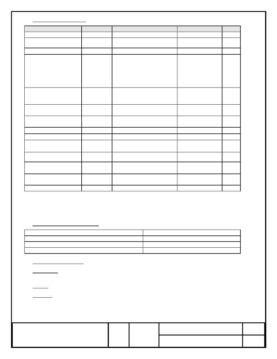
3.1.1 Electrical Characteristics
PARAMETER
SYMBOL
CONDITIONS
VALUE
UNIT
Frequency Nom.
fo
-
2. to 90
MHz
Supply voltage, Nom.
Vs
Vs±5%
See part number
generation table
V
Input Current, max.
Is
Vs, nom. / Ta=+25°C
50
mA
Overall Frequency stability
(including Operating
Temperature, ±5% Load
Change, ±5% Supply
Voltage change, 10 year
aging, and radiation)
Δf/fc (Ta)
Contact factory for other
options available
See part number
generation table
ppm
Voltage Control Range For
Frequency Adjustment
Min.
Vc
DC
See part number
generation table
Volts
Control Voltage at which
fo will occur at 25°C
Vc/fo
DC
½Vc ±0.5
Volts
Frequency
Pulling
range,
Min
Δf/Vc
Over the voltage control range
See part number
generation table
ppm
Linearity, max.
Δf/V
-
10
%
Input impedance, min.
Zin
-
10.0
KΩ
Modulation freq.
bandwidth, min.
MBW (-3dB)
Vs, nom. / Ta=+25°C Vc/fo,
and 50Ω load
10.0
KHz
Output
VOH / VOL load=15pF, Vcc=nom.
0.9•Vcc / 0.1•Vcc
V
Duty cycle
DC
load=15pF/ @50%Vcc,
Ta=+25°C
See part number
generation table
%
Rise- / fall time
tr / tf
20%~80% Vout, 80%~20%
Vout
.5…7 (see note A)
nSec
Load
15
pF
A:
Supply Current, rise & fall time are frequency dependent
3.2
Absolute Maximum Rating
Supply Voltage
0 to +6.0 VDC
DC Input Current
50 mA maximum
Storage Temperature range
-62°C to +125°C
Lead Temperature (Soldering, 10 seconds)
300°C
3.2.1 Physical Characteristics
3.2.1.1 Dimensions - The VCXO outline dimensions and terminal connections shall be as shown in Figure 1
herein.
3.2.1.2 Weight - The VCXO shall weigh less than or equal to 15 grams.
3.2.1.3 Materials - The VCXO package body and lead finish shall be gold in accordance with MIL-PRF-38534.