Q-tech, Qt93w and qt93p series, Thermal characteristics – Q-Tech QT93 User Manual
Page 5: Phase noise and phase jitter integration
5
Q-TECH Corporation - 10150 W. Jefferson Boulevard, Culver City 90232 - Tel: 310-836-7900 - Fax: 310-836-2157 - www.q-tech.com
QT93W and QT93P SERIES
HIGH-RELIABILITY LVPECL OR LVDS MINIATURE CLOCK OSCILLATORS
2.5 to 3.3Vdc - 40MHz to 320MHz
Q-TECH
CORPORATION
QT93W & P (Revision E, October 2010) (ECO #10000)
45º
45º
Hybrid Case
Substrate
Die
D/A epoxy
D/A epoxy
Heat
Die
R1
D/A epoxy
Substrate
D/A epoxy
Hybrid Case
R2
R3
R4
R5
Thermal Characteristics
JA
JC
CA
Die
T
T
T
C
A
J
CA
JC
(Figure 2)
(Figure 1)
(Figure 3)
The heat transfer model in a hybrid package is described in
figure 2.
Heat spreading occurs when heat flows into a material layer of
increased cross-sectional area. It is adequate to assume that
spreading occurs at a 45° angle.
The total thermal resistance is calculated by summing the
thermal resistances of each material in the thermal path
between the device and hybrid case.
RT = R1 + R2 + R3 + R4 + R5
The total thermal resistance RT (see figure 3) between the heat
source (die) to the hybrid case is the Theta Junction to Case
(Theta JC) in°C/W.
• Theta junction to case (Theta JC) for this product is 35°C/W.
• Theta case to ambient (Theta CA) for this part is 100°C/W.
• Theta Junction to ambient (Theta JA) is 135°C/W.
Maximum power dissipation PD for this package at 25°C is:
• PD(max) = (TJ (max) – TA)/Theta JA
• With TJ = 175°C (Maximum junction temperature of die)
• PD(max) = (175 – 25)/135 = 1.11W
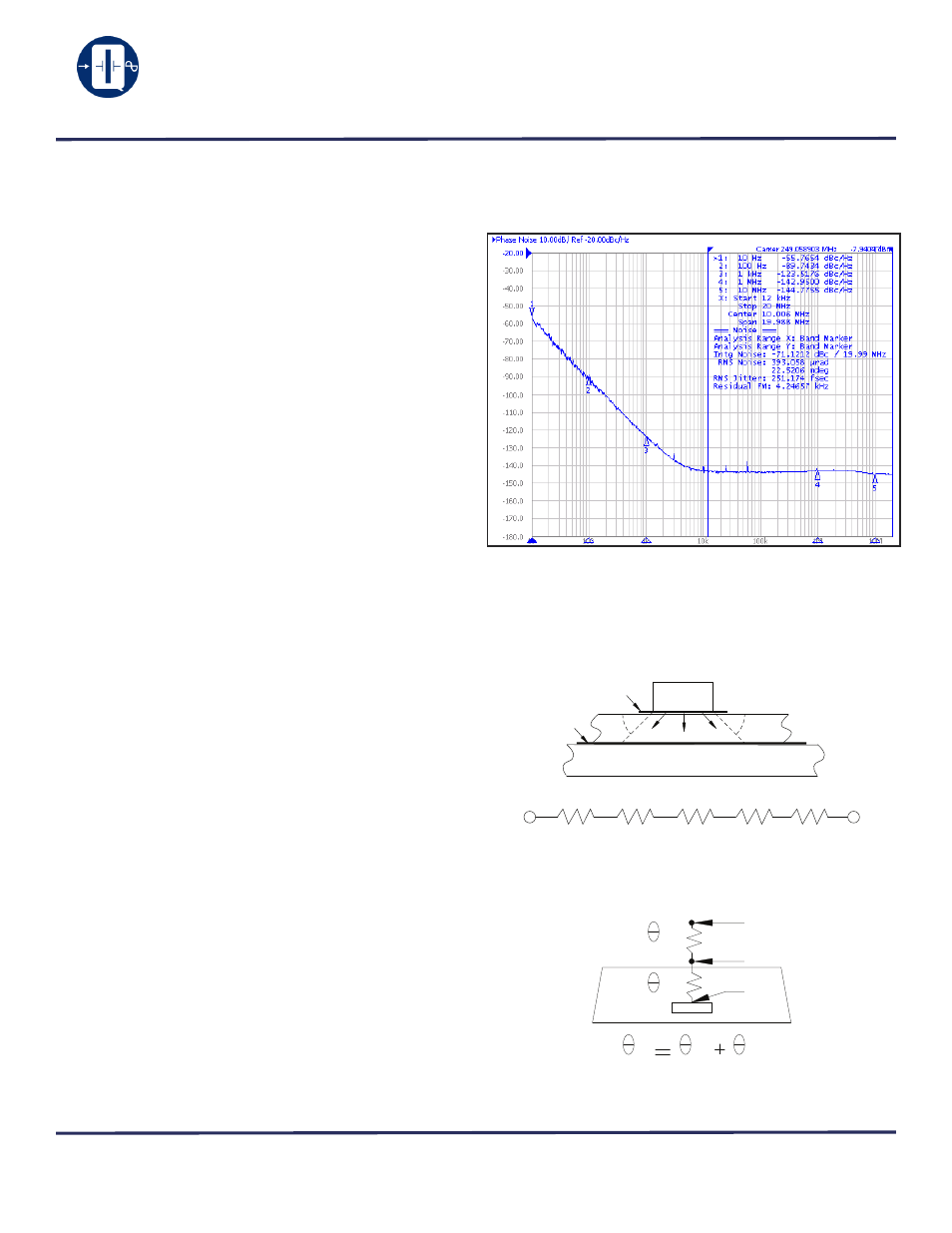
Phase Noise and Phase Jitter Integration
Phase noise is measured in the frequency domain, and is
expressed as a ratio of signal power to noise power measured
in a 1Hz bandwidth at an offset frequency from the carrier, e.g.
10Hz, 100Hz, 1kHz, 10kHz, 100kHz, etc. Phase noise meas-
urement is made with an Agilent E5052A Signal Source Ana-
lyzer (SSA) with built-in outstanding low-noise DC power
supply source. The DC source is floated from the ground and
isolated from external noise to ensure accuracy and repeatabil-
ity.
In order to determine the total noise power over a certain
frequency range (bandwidth), the time domain must be
analyzed in the frequency domain, and then reconstructed in
the time domain into an rms value with the unwanted frequen-
cies excluded. This may be done by converting L(f) back to
Sφ(f) over the bandwidth of interest, integrating and perform-
ing some calculations.
The value of RMS jitter over the bandwidth of interest, e.g.
10kHz to 20MHz, 10Hz to 20MHz, represents 1 standard devi-
ation of phase jitter contributed by the noise in that defined
bandwidth.
Figure 1 shows a typical Phase Noise/Phase jitter of a
QT93LW, 3.3Vdc, 250MHz clock at offset frequencies 10Hz to
10MHz, and phase jitter integrated over the bandwidth of
12kHz to 20MHz.