Low-voltage start-up oscillator (boot pin), Bootstrapped/non-bootstrapped modes – Rainbow Electronics MAX863 User Manual
Page 9
MAX863
Dual, High-Efficiency, PFM, Step-Up
DC-DC Controller
_______________________________________________________________________________________
9
Low-Voltage Start-Up Oscillator
(BOOT Pin)
The MAX863 features a low-voltage start-up oscillator
that guarantees start-up in bootstrapped configuration
down to 1.5V. At these low supply voltages, the error
comparator and internal biasing of the IC are locked
out. The low-voltage oscillator switches the external
MOSFET with around 30% duty cycle until the voltage
at V
DD
rises above 2.7V. At this point, the error com-
parator and one-shot timing circuitry turn on. The low-
voltage oscillator is enabled by connecting the BOOT
pin to V
DD
. When BOOT is high, V
DD
must be connect-
ed to V
OUT1
.
Use the start-up oscillator in the bootstrapped configu-
ration only, since the MAX863 operates in an open-loop
state while the start-up oscillator is active. When using
a non-bootstrapped circuit configuration, connect
BOOT to GND to disable the start-up oscillator. This
prevents the output from rising too high when V
DD
is
between 1.5V and 2.7V, such as during power-up and
low-battery conditions.
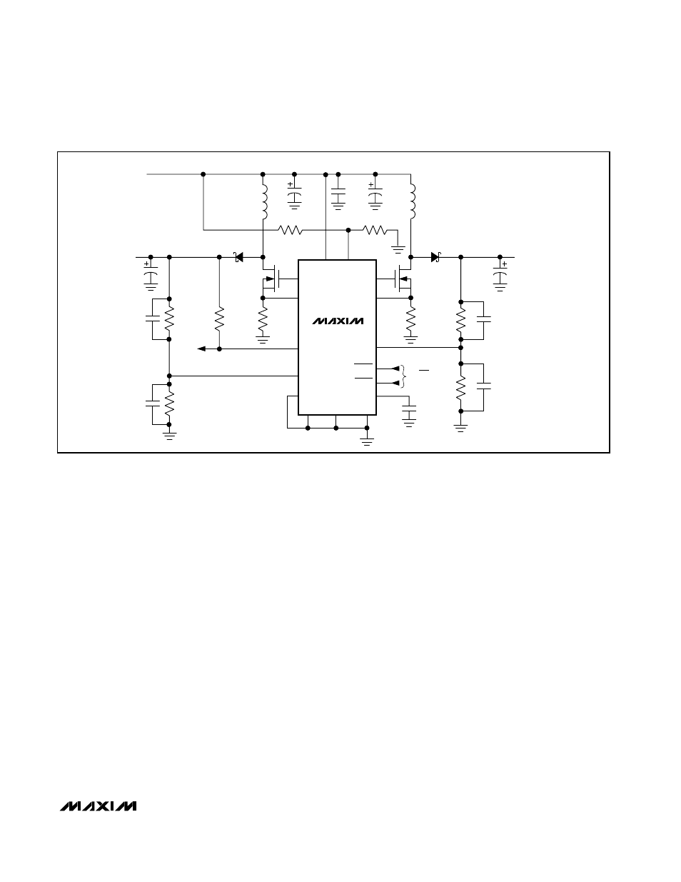
Bootstrapped/Non-Bootstrapped Modes
Figures 2 and 4 show standard applications in boot-
strapped and non-bootstrapped modes. In boot-
strapped mode, the IC is powered from the output (V
DD
is connected to OUT1, BOOT is connected to V
DD
).
Bootstrapped-mode operation is useful for increasing
the gate drive to the MOSFETs in low-input-voltage
applications, since EXT1 and EXT2 swing from V
DD
to
GND. Increasing the gate-drive voltage reduces MOS-
FET on-resistance, which improves efficiency and
increases the load range. For supply voltages below
5V, bootstrapped mode is recommended. In boot-
strapped mode, the output connected to V
DD
must not
exceed 11V. If BOOT is high, V
DD
must be connect-
ed to OUT1.
In non-bootstrapped mode, the IC is powered by a
direct connection from the input voltage to V
DD
. Since
the voltage swing applied to the gate of the external
MOSFET is derived from V
DD
, the external MOSFET on-
resistance increases at low input voltages. The mini-
mum input voltage is 2.7V. For operation down to 4V,
use logic-level MOSFETs. For lower input voltages, use
low-threshold logic-level MOSFETs. When both output
voltages are set above 11V, non-bootstrapped mode is
mandatory.
MAX863
EXT2
CS2
V
OUT2
= 24V
V
OUT1
= 12V
V
IN
= 2.7V TO 11V
N1.B
IRF7301
C7
0.1
µF
R4
56k
1%
C6
15pF
C5
22
µF
35V
0.1
Ω
R2
100m
Ω
R3
1M
1%
N1.A
R1
50m
Ω
R7
100k
C1
100
µF
16V
≤0.1Ω
R8
1M
1%
R9
115k
1%
D1
MBRS340T3
R6
R5
C8
10pF
D2
MBRS140
L1
10
µH
2A
L2
10
µH
1A
C3
100
µF
20V
≤0.1Ω
C4
100
µF
20V
≤0.1Ω
C2
0.1
µF
FB2
SHDN1
EXT1
CS1
LBO
LOW-BATTERY
DETECTOR OUTPUT
FB1
V
DD
PGND
LBI
GND
BOOT
SENSE1
SHDN2
REF
ON/OFF
C10
270pF
C9
82pF
Figure 4b. Adjustable Non-Bootstrapped Typical Operating Circuit