Rainbow Electronics MAX863 User Manual
Page 14
MAX863
Dual, High-Efficiency, PFM, Step-Up
DC-DC Controller
14
______________________________________________________________________________________
Set Feedback Compensation
External voltage feedback to the MAX863 should be
compensated for stray capacitance and EMI in the
feedback network. Proper compensation is achieved
when the MAX863 switches evenly, rather than in wide-
ly spaced bursts of pulses with large output ripple.
Typically, lead compensation consisting of a 10pF to
220pF ceramic capacitor (C1 in Figure 7) across the
upper feedback resistor is adequate. Circuits with
V
OUT
or V
DD
greater than 7.5V may require a second
capacitor across the lower feedback resistor. Initially,
choose this capacitor so that R2C2 = R1C1. Set the
final values of the compensation capacitors based on
empirical analysis of a prototype.
PC Board Layout and Routing
High switching speeds and large peak currents make
PC board layout an important part of design. Poor lay-
out can cause excessive EMI and ground-bounce, both
of which can cause instability or regulation errors by
corrupting the voltage and current-feedback signals.
Place power components as close together as possi-
ble, and keep their traces short, direct, and wide. Keep
the extra copper on the board and integrate it into
ground as an additional plane. On multi-layer boards,
avoid interconnecting the ground pins of the power
components using vias through an internal ground
plane. Instead, place the ground pins of the power
components close together and route them in a “star”
ground configuration using component-side copper,
then connect the star ground to the internal ground
plane using multiple vias.
The current-sense resistor and voltage-feedback net-
works should be very close to the MAX863. Noisy
traces, such as from the EXT pins, should be kept away
from the voltage-feedback networks and isolated from
them using grounded copper. Consult the MAX863
evaluation kit manual for a full PC board example.
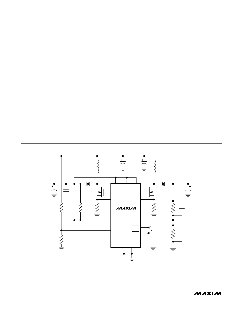
MAX863
EXT2
CS2
V
OUT2
= 24V, 35mA
V
OUT1
= 5V
V
IN
= 1.8V TO V
OUT1
N1B
IRF7103
C7
0.1
µF
R4
49.9k
1%
C6
15pF
C5
22
µF
35V
0.1
Ω
R2
100m
Ω
R3
909k
1%
N1A
R1
50m
Ω
R7
100k
C1
220
µF
10V
≤0.1Ω
R5
R6
D1
MBRS340T3
D2
MBRS140
L1
10
µH
2A
L2
10
µH
1A
C3
100
µF
10V
≤0.1Ω
C4
100
µF
10V
≤0.1Ω
C2
0.1
µF
ON/OFF
FB2
SHDN1
EXT1
CS1
LBO
LOW-BATTERY
DETECTOR OUTPUT
LBI
SENSE1
V
DD
BOOT
GND
SHDN2
REF
PGND
FB1
C8
270pF
Figure 8. Bootstrapped 3.3V Logic and 24V LCD Bias Supply