Rainbow Electronics MAX863 User Manual
Page 7
MAX863
Dual, High-Efficiency, PFM, Step-Up
DC-DC Controller
_______________________________________________________________________________________
7
Continuous/Discontinuous-Conduction
Modes
Each converter in the MAX863 determines from moment
to moment whether to switch or not, waiting until the out-
put voltage drops before initiating another cycle. Under
light loads, the inductor current ramps to zero before the
next cycle; this is discontinuous-conduction mode.
Continuous-conduction mode occurs when the next
switching cycle begins while current is still flowing
through the inductor. The transition point between dis-
continuous- and continuous-conduction mode is deter-
mined by input and output voltages, and by the size of
the inductor relative to the peak switching current. In
general, reducing inductance toward the minimum rec-
ommended value pushes the transition point closer to
the maximum load current. If the inductor value is low
enough or the output/input voltage ratio high enough,
the DC-DC converter may remain in discontinuous-con-
duction mode throughout its entire load range.
The MAX863 transitions into continuous-conduction
mode in two ways, depending on whether preset or
adjustable mode is used and how the external feed-
back network is compensated. Under light loads, the IC
switches in single pulses (Figure 3a). The threshold of
transition into continuous-conduction mode is reached
when the inductor current waveforms are adjacent to
one another, as shown in Figure 3b. As the load
increases, the transition into continuous-conduction
mode progresses by raising the minimum inductor cur-
rent (Figures 3c, 3d). Depending on feedback compen-
sation, transition into continuous-conduction mode may
also progress with grouped pulses (Figures 3e, 3f).
Pulse groups should be separated by less than two or
three switching cycles. Output ripple should not be
significantly more than the single-cycle no-load case.
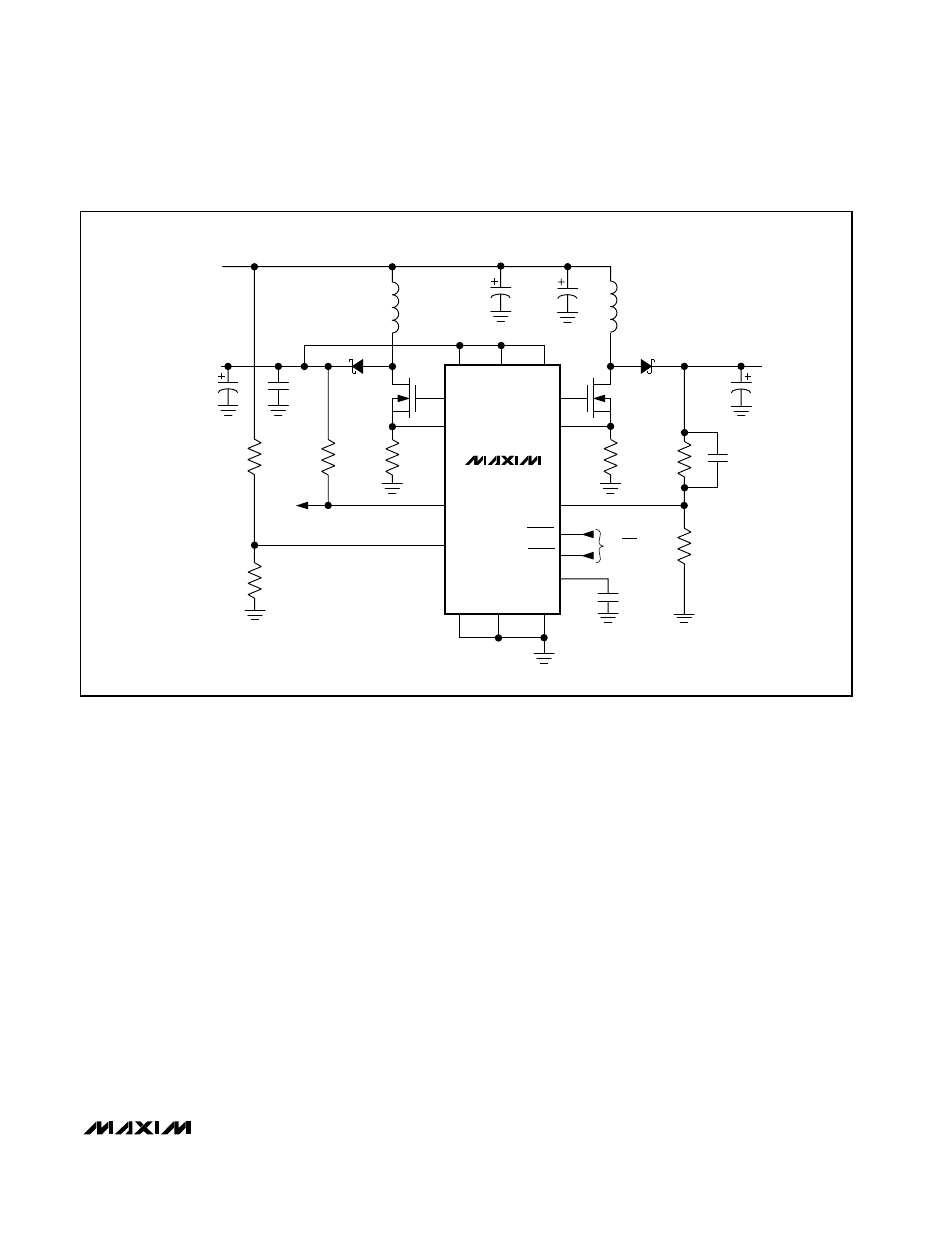
MAX863
EXT2
CS2
V
OUT2
= 3.3V
V
OUT1
= 5V
V
IN
= 1.5V TO THE LOWER OF V
OUT1
OR V
OUT2
N1B
IRF7301
C7
0.1
µF
R4
100k
1%
C6
10pF
C5
330
µF
10V
≤0.1Ω
R2
50m
Ω
R3
165k
1%
N1A
R1
50m
Ω
R7
100k
C1
220
µF
10V
≤0.1Ω
R5
R6
C2
0.1
µF
D1
MBRS340T3
D2
MBRS340T3
L1
10
µH
2A
L2
10
µH
2A
C3
100
µF
10V
≤0.1Ω
C4
100
µF
10V
≤0.1Ω
ON/OFF
FB2
SHDN1
EXT1
CS1
LBO
LOW-BATTERY
DETECTOR OUTPUT
LBI
SENSE1
V
DD
PGND
BOOT
GND
FB1
SHDN2
REF
Figure 2. Bootstrapped Typical Operating Circuit