W-cdma lna/mixer ics, Detailed description, Pin description – Rainbow Electronics MAX2389 User Manual
Page 8
MAX2387/MAX2388/MAX2389
Detailed Description
The MAX2387/MAX2388/MAX2389 include an LNA
and downconverter mixer. These devices feature a
shutdown mode to power down the IC during the front-
end receiver’s idle periods. Each IC operates from a
+2.7V to +3.3V single supply and is housed in a 12-pin
ultra-small QFN (3mm
✕
3mm) leadless package.
The MAX2387/MAX2388/MAX2389 are fabricated using
an advanced high-frequency silicon germanium
process. The LNA and mixer NF and IIP3 have been
optimized to provide excellent RF performance in the
2110MHz to 2170MHz band, while drawing minimal
current.
For the MAX2387/MAX2388, the mixer’s performance is
optimized for a -10dBm typical drive at the LO buffer
input port. The MAX2389’s mixer performance is opti-
mized for a -4dBm typical drive at the LO input port.
The LO port for all versions can be driven either single-
ended or differentially.
LNA High/Low-Gain Mode
These devices offer two modes of operation for the LNA:
high-gain mode and low-gain mode, selectable with a
GAIN select pin. The MAX2387 has a gain of 15dB in
high-gain mode and -16.6dB in low-gain mode. The
MAX2388/MAX2389 have a gain of 15dB in high-gain
mode and -2.8dB in low-gain mode. Matching LNA in
high-gain mode will ensure matching in low-gain mode.
Downconverter Mixer
The receive mixer is a wideband, single-balanced
design with exceptional noise figure and linearity. The
LO input frequency range is 2330MHz to 2360MHz and
the RF input frequency range is 2110MHz to 2170MHz.
The mixer is internally matched to 50
Ω, thus eliminating
any external matching components.
LO Input Buffers
The MAX2387/MAX2388 feature open-collector LO
buffers to increase isolation between the LO and the
rest of the system. The MAX2389 offers a lower current
consumption for applications that do not require an LO
buffer.
RF Inputs
The MIX_IN input is typically connected to the LNA out-
put through an off-chip filter providing image rejection
and out-of-band interferers filtering. The LNA input and
output require an external matching network to 50
Ω.
Note that the mixer input is internally matched to 50
Ω.
See Figure 1, Typical Application Circuits for 2.14GHz.
LO Inputs
The LO+ and LO- pins are internally terminated with
100
Ω resistors. AC-couple the local-oscillator signal to
these pins. If a single-ended LO source is used, con-
nect LO+ to ground using an AC-coupling capacitor.
W-CDMA LNA/Mixer ICs
8
_______________________________________________________________________________________
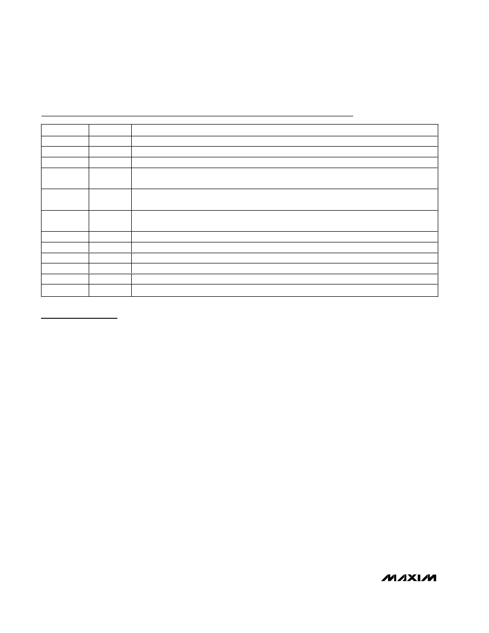
Pin Description
PIN
NAME
FUNCTION
1
LNA_OUT
RF Output Port for LNA. Requires external matching.
2
GAIN
LNA/Mixer Gain Control Input
3
MIX_IN
RF Input Port for Mixer. Internally matched to 50
Ω.
4
SHDN
Shutdown Input. Drive low to enable shutdown mode. Drive high or connect to V
CC
for normal
operation.
5
LO+
Noninverting LO Input for LO Buffer (MAX2387/MAX2388) or Mixer (MAX2389). Differential input
impedance is 200
Ω. AC-couple to GND when the LO is driven single-endedly.
6
LO-
Inverting LO Input for LO Buffer (MAX2387/MAX2388) or Mixer (MAX2389). Differential input
impedance is 200
Ω.
7
IF-
Inverting Mixer’s IF Open-Collector Output
8
IF+
Noninverting Mixer’s IF Open-Collector Output
9
V
CC
Supply Voltage (+2.7V to +3.3V). Capacitively bypass to GND near the IC.
10
LNA_IN
RF Input Port for LNA. Requires external matching.
11
GND
Ground
12
BIAS
LNA/Mixer Bias Pin. For nominal bias, connect 24k
Ω ±1% resistor to GND.