Functional description – Rainbow Electronics LM81 User Manual
Page 15

Functional Description
(Continued)
3.5 Reading Conversion Results
The conversion results are available in the Value RAM.
Conversions can be read at any time and will provide the
result of the last conversion. Because the ADC stops, and
starts a new conversion whenever it is read, reads of any
single value should not be done more often than once every
56 ms. When reading all values, allow at least 0.82 seconds
between reading groups of values. Reading more frequently
than once every 0.82 seconds can also prevent complete
updates of Interrupt Status Registers and Interrupt Output’s.
A typical sequence of events upon power on of the LM81
would consist of:
1.
Set WATCHDOG Limits
2.
Set Interrupt Masks
3.
Start the LM81 monitoring process
3.6 Digital Communication Noise Considerations
The SMBData and SMBCLK logic input levels were changed
in the SMBus 1.1 specification. SMBus 1.0 levels were set to
1.4V for a logic high and 0.6V for a logic low. In SMBus 1.1
they were changed to 2.1V for a logic high and 0.8V for a
logic low. Devices that meet the SMBus 1.0 specification
have issues in that the logic levels did not allow for enough
noise immunity for some pcb layouts. This has changed with
the SMBus 1.1 specification because the higher logic levels
allow for more hysteresis in the schmitt trigger inputs stages
and thus more noise immunity. It may be required in some
cases to add a series 5.1k
Ω
resistor connected at the SM-
BCLK pin of the LM81C to improve its noise immunity. In
addition to meeting the SMBus 1.1 logic levels, the LM81B
has a built-in glitch filter that rejects 100MHz or greater to
make it impervious to noise.
4.0 ANALOG INPUTS
All analog input voltages are digitized to 8-bits of resolution.
All analog inputs, except for Vccp1 and Vccp2, include inter-
nal resistor attenuators. The theoretical LSB size, theoretical
voltage input required for an ADC reading of 192 (3/4 scale)
and 255 (full scale) for each analog input is detailed in the
table below:
Input
LSB size
Vin for
192
Vin for
255
2.5 Vin
13 mV
2.5V
3.320V
3.3 Vin
17.2 mV
3.3V
4.383V
5 Vin
26 mV
5V
6.641V
12 Vin
62.5 mV
12V
15.93V
Vccp1, Vccp2
14.1 mV
2.7V
3.586V
Thus monitoring power supplies within a system can be
easily accomplished by tying the Vccp, +2.5 Vin, +3.3 Vin,
+5 Vin and +12 Vin analog inputs to the corresponding
system supply. A digital reading can be converted to a volt-
age by simply multiplying the decimal value of the reading by
the LSB size.
For inputs with attenuators the input impedance is greater
than 90 k
Ω
. Vccp inputs do not have resistor attenuators and
are are directly tied to the ADC, therefore having a much
larger input impedance.
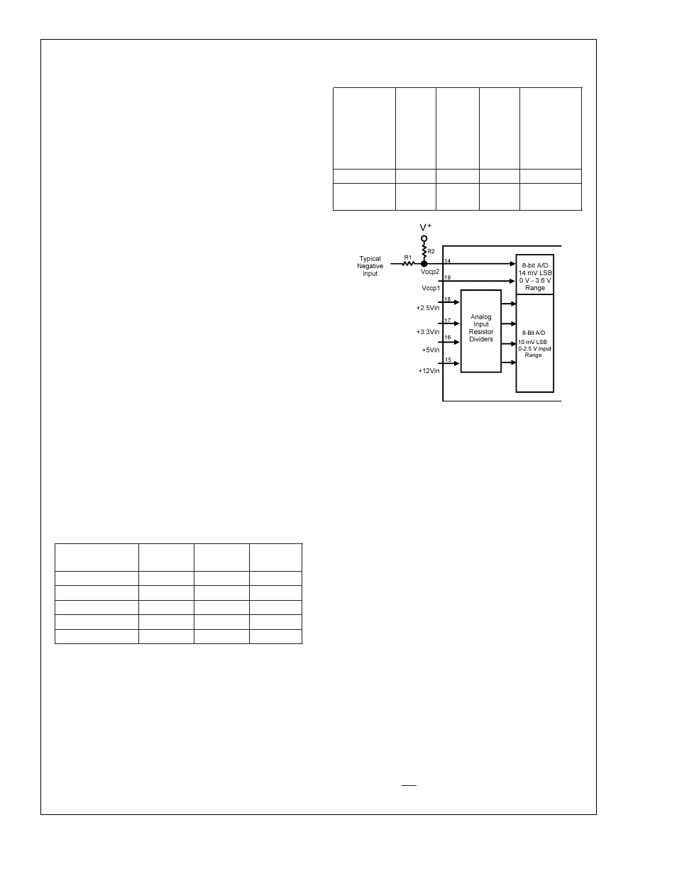
A negative power supply voltage can be applied to a Vccp
input through a resistor divider referenced to a known posi-
tive DC voltage as show in
Figure 6. The resistor values
shown in the table below for the circuit of Figure 6 will
provide approximately 1.25V at the Vccp analog inputs of the
LM81 for a nominal reading of 89.
Voltage
Measure-
ments
(V
S
)
R2
R1
V
+
Voltage
at
Analog In-
puts
(ADC code
89)
−12V
40 k
Ω
141 k
Ω
+5V
+1.25V
−5V
40 k
Ω
66.7
k
Ω
+5V
+1.25V
The resistors were selected by setting R2 = 40 k
Ω
and then
calculating R2 using the following equation:
R1 = [(1.25V − V
S
) ÷ (V
+
− 1.25V)] x 40 k
Ω
The maximum R1 can be is restricted by the DC input
current of a Vccp input.
Inputs with internal resistor dividers (+2.5 Vin, +3.3 Vin or
+5 Vin, +12 Vin) can have voltage applied that exceeds the
power supply up to: 3.6V for +2.5 Vin, 4.6V for +3.3 Vin, 6.8V
for +5 Vin, and 15V for +12 Vin. The Vccp inputs have a
parasitic diode to the positive supply, so care should be
taken not to forward bias this diode. All analog inputs have
internal diodes that clamp the input voltage when going
below ground thus limiting the negative analog input voltage
range to −50 mV. Violating the analog input voltage range of
any analog input has no detrimental effect on the other
analog inputs. External resistors should be included to limit
input currents to the values given in the ABSOLUTE MAXI-
MUM RATINGS for Input Current At Any Pin whenever ex-
ceeding the analog input voltage range, even on an
un-powered LM81. Inputs with external attenuator networks
will usually meet these requirements. If it is possible for
inputs without attenuators (such as Vccp1 and Vccp2) to be
turned on while LM81 is powered off, additional resistors of
about 10 k
Ω
should be added in series with the inputs to limit
the input current.
4.1 Analog Input Interrupts
A WATCHDOG window comparison on the analog inputs
can activate the INT interrupt output. A converted input volt-
age that is above its respective HIGH limit or less than or
DS100072-11
FIGURE 6. Input Examples. Resistor values shown in
table provide approximately 1.25V at the Vccp inputs.
LM81
www.national.com
15
