Detailed description, Applications information, Pin description – Rainbow Electronics MAX2641 User Manual
Page 5
MAX2640/MAX2641
400MHz to 2500MHz SiGe
Ultra-Low-Noise Amplifiers
_______________________________________________________________________________________
5
Detailed Description
The MAX2640 and MAX2641 are ultra-low-noise ampli-
fiers that operate with RF input frequency ranges of
400MHz to 1500MHz (MAX2640) or 1400MHz to
2500MHz (MAX2641). These devices are available in
SOT23-6 packages and contain internal bias circuitry to
minimize the number of required external components.
Their small size and low external component count
make them ideal for applications where board space is
limited.
Applications Information
External Matching Components
The MAX2640/MAX2641 are easy to use, generally
requiring only five external components as shown in the
Typical Operating Circuit
. To reduce external compo-
nent count further, replace external inductors with
microstrip transmission lines. The high reverse isolation
allows the tuning of the input matching network without
affecting the output match, and vice versa. Select input
and output matching networks to obtain the desired
combination of gain, noise figure, and return loss per-
formance. The
Typical Operating Circuits
show the rec-
ommended input and output matching networks for
the MAX2640/MAX2641 at 900MHz and 1900MHz,
respectively. These values are optimized for best
simultaneous gain, noise figure, and return loss perfor-
mance. To aid in the design of matching networks for
other frequencies, Tables 1 and 2 list typical device S-
parameters and Tables 3 and 4 list typical device noise
parameters.
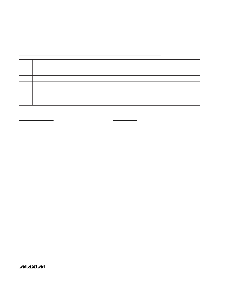
NAME
FUNCTION
1
RFIN
Amplifier Input. AC-couple to this pin with a DC blocking capacitor. Use recommended input matching
network (see
Typical Operating Circuit
).
2, 3, 5
GND
Ground. For optimum performance, provide a low inductance connection to the ground plane.
PIN
4
RFOUT
Amplifier Output. Use the recommended series blocking or matching capacitor (see
Typical Operating
Circuit
).
6
V
CC
Supply Voltage. Bypass to ground directly at the supply pin. The value of the bypass capacitor is deter-
mined by the lowest operating frequency. Additional bypassing may be necessary for long V
CC
lines (see
Typical Operating Circuit
).
Pin Description