Rf electrical characteristics – Rainbow Electronics MAX2641 User Manual
Page 2
MAX2640/MAX2641
400MHz to 2500MHz SiGe
Ultra-Low-Noise Amplifiers
2
_______________________________________________________________________________________
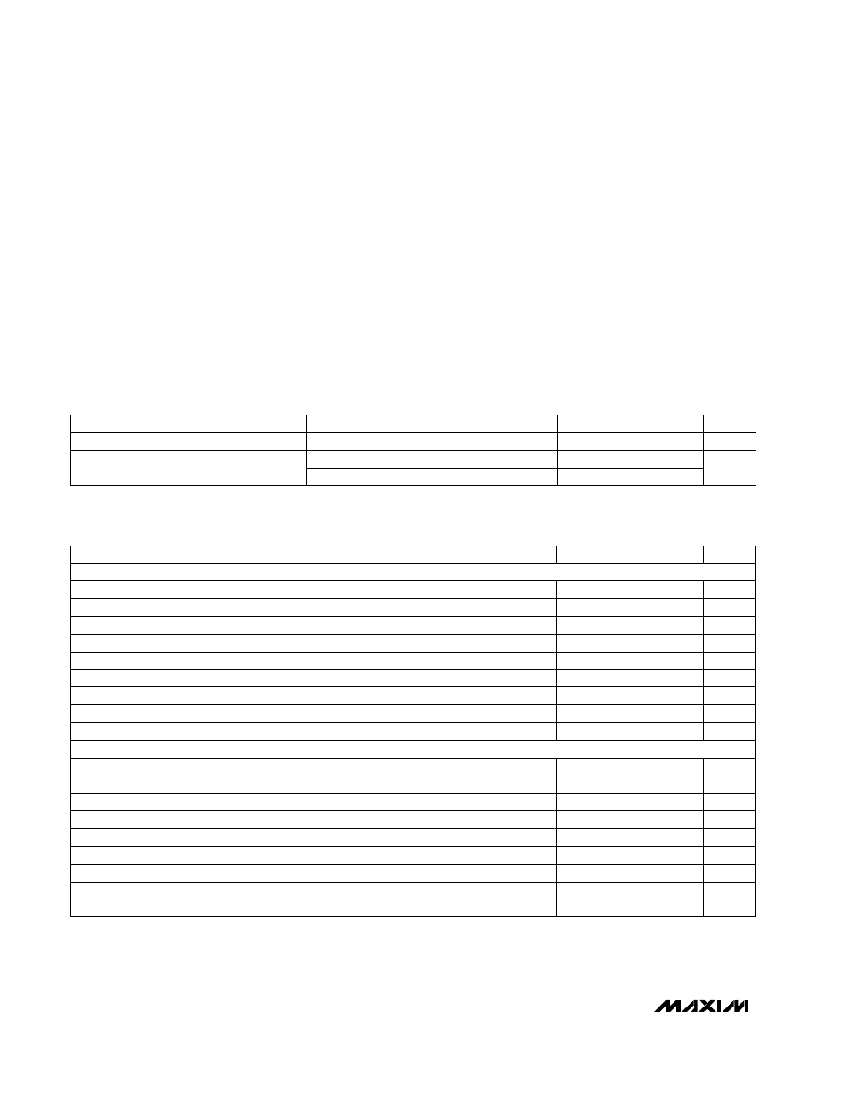
ABSOLUTE MAXIMUM RATINGS
DC ELECTRICAL CHARACTERISTICS
(V
CC
= +2.7V to +5.5V, T
A
= T
MIN
to T
MAX,
unless otherwise noted. Typical values are at V
CC
= +3.0V, T
A
= +25°C.)
Stresses beyond those listed under “Absolute Maximum Ratings” may cause permanent damage to the device. These are stress ratings only, and functional
operation of the device at these or any other conditions beyond those indicated in the operational sections of the specifications is not implied. Exposure to
absolute maximum rating conditions for extended periods may affect device reliability.
V
CC
to GND .............................................................-0.3V to +6V
RFIN Power (50
Ω
source) (Note 1) ..................................+5dBm
Continuous Power Dissipation (T
A
= +70°C)
SOT23-6 (derate 8.7mW/°C above +70°C)..................696mW
Operating Temperature Range ...........................-40°C to +85°C
Maximum Junction Temperature .....................................+150°C
Storage Temperature Range .............................-65°C to +160°C
Lead Temperature (soldering, 10sec) .............................+300°C
T
A
= +25°C
CONDITIONS
mA
3.5
4.7
V
2.7
5.5
Operating Supply Voltage
Operating Supply Current
UNITS
MIN
TYP
MAX
PARAMETER
(Note 6)
(Note 5)
(Note 4)
T
A
= T
MIN
to T
MAX
T
A
= T
MIN
to T
MAX
(Note 4)
CONDITIONS
dBm
-4
Input Third-Order Intercept Point
dBm
-21
Input 1dB Gain Compression Point
dB
30
Reverse Isolation
dB
-12
Output Return Loss
dB
-12
Input Return Loss
dB
1.3
1.5
Noise Figure
dB
0.9
2.4
Gain Variation Over Temperature
dB
12.4
14.4
Gain
MHz
1400
2500
RFIN Frequency Range
dB
12.8
15.1
Gain
MHz
400
1500
RFIN Frequency Range
dBm
-10
Input Third-Order Intercept Point
dBm
-22
Input 1dB Gain Compression Point
dB
40
Reverse Isolation
dB
0.6
1.7
Gain Variation Over Temperature
dB
0.9
1.1
Noise Figure
dB
-11
Input Return Loss
dB
-14
Output Return Loss
UNITS
MIN
TYP
MAX
PARAMETER
RF ELECTRICAL CHARACTERISTICS
(V
CC
= +3.0V, P
RFIN
= -34dBm, Z
O
= 50
Ω
, T
A
= +25°C, unless otherwise noted.) (Notes 2 and 3)
MAX2640 (f
RFIN
= 900MHz)
MAX2641 (f
RFIN
= 1900MHz)
Note 1:
Pin must be AC-coupled with a DC blocking capacitor.
T
A
= -40°C to +85°C
6.4