Rainbow Electronics MAX920 User Manual
Page 2
MAX917–MAX920
SOT23, 1.8V, Nanopower, Beyond-the-Rails
Comparators With/Without Reference
2
_______________________________________________________________________________________
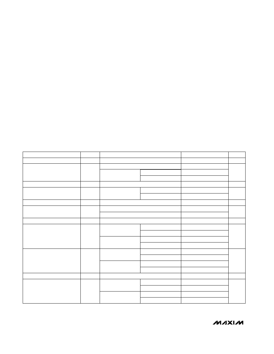
ABSOLUTE MAXIMUM RATINGS
ELECTRICAL CHARACTERISTICS—MAX917/MAX918
(V
CC
= +5V, V
EE
= 0, V
IN+
= V
REF
, T
A
= -40°C to +85°C, unless otherwise noted. Typical values are at T
A
= +25°C.) (Note 1)
Stresses beyond those listed under “Absolute Maximum Ratings” may cause permanent damage to the device. These are stress ratings only, and functional
operation of the device at these or any other conditions beyond those indicated in the operational sections of the specifications is not implied. Exposure to
absolute maximum rating conditions for extended periods may affect device reliability.
Supply Voltage (V
CC
to V
EE
)..................................................+6V
Voltage Inputs (IN+, IN-, REF) .........(V
EE
- 0.3V) to (V
CC
+ 0.3V)
Output Voltage
MAX917/MAX919 ........................(V
EE
- 0.3V) to (V
CC
+ 0.3V)
MAX918/MAX920 ......................................(V
EE
- 0.3V) to +6V
Output Current..................................................................±50mA
Output Short-Circuit Duration .............................................10sec
Continuous Power Dissipation (T
A
= +70°C)
5-Pin SOT23 (derate 7.31mW/°C above +70°C).........571mW
8-Pin SO (derate 5.88mW/°C above +70°C)...............471mW
Operating Temperature Range ...........................-40°C to +85°C
Storage Temperature Range .............................-65°C to +150°C
Lead Temperature (soldering, 10sec) .............................+300°C
V
CC
= 1.8V
V
CC
= 1.8V
V
CC
= 5V
V
CC
= 1.8V
V
CC
= 5V
Output Voltage Swing Low
V
OL
190
400
mV
500
55
200
T
A
= T
MIN
to T
MAX
T
A
= +25°C
300
V
CC
= 5V,
I
SINK
= 8mA
T
A
= T
MIN
to T
MAX
V
CC
= 1.8V,
I
SINK
= 1mA
T
A
= +25°C
T
A
= T
MIN
to T
MAX
T
A
= +25°C
T
A
= T
MIN
to T
MAX
T
A
= +25°C
T
A
= T
MIN
to T
MAX
T
A
= +25°C
T
A
= T
MIN
to T
MAX
T
A
= +25°C
T
A
= T
MIN
to T
MAX
T
A
= +25°C
PARAMETER
SYMBOL
MIN
TYP
MAX
UNITS
10
Input Offset Voltage
V
OS
1
5
mV
IN+ Voltage Range
V
IN+
V
EE
- 0.2
V
CC
+ 0.2
V
1.60
Input-Referred Hysteresis
V
HB
4
mV
Input Bias Current
I
B
0.15
1
nA
2
Power-Supply Rejection Ratio
PSRR
0.1
1
mV/V
Supply Current
Supply Voltage Range
V
CC
1.8
5.5
V
I
CC
0.75
µA
0.80
1.30
Output Voltage Swing High
V
CC
- V
OH
190
400
mV
500
55
200
300
Output Leakage Current
I
LEAK
0.001
1
µA
Output Short-Circuit Current
I
SC
95
mA
8
98
10
CONDITIONS
MAX917 only, V
CC
=
5V, I
SOURCE
= 8mA
(Note 2)
Inferred from the output swing test
(Note 3)
MAX917 only, V
CC
=
1.8V, I
SOURCE
= 1mA
V
CC
= 1.8V to 5.5V
MAX918 only, V
O
= 5.5V
Sourcing, V
O
= V
EE
Inferred from the PSRR test
Sinking, V
O
= V
CC
V
CC
= 5V