Typical application circuit, Pin configurations (continued), Board layout and bypassing – Rainbow Electronics MAX920 User Manual
Page 12: Zero-crossing detector, Logic-level translator
MAX917–MAX920
SOT23, 1.8V, Nanopower, Beyond-the-Rails
Comparators With/Without Reference
Maxim cannot assume responsibility for use of any circuitry other than circuitry entirely embodied in a Maxim product. No circuit patent licenses are
implied. Maxim reserves the right to change the circuitry and specifications without notice at any time.
12
____________________Maxim Integrated Products, 120 San Gabriel Drive, Sunnyvale, CA 94086 408-737-7600
© 1999 Maxim Integrated Products
Printed USA
is a registered trademark of Maxim Integrated Products.
MAX920
IN-
100k
100k
R
PULL-UP
3V (5V)
LOGIC OUT
OUT
V
CC
+5V (+3V)
+3V (+5V)
V
EE
5V (3V) LOGIC IN
IN+
LOGIC LEVEL
TRANSLATOR
V
EE
V
CC
OUT
R3
R2
R1
R4
V
REF
V
IN
V
CC
MAX918
MAX920
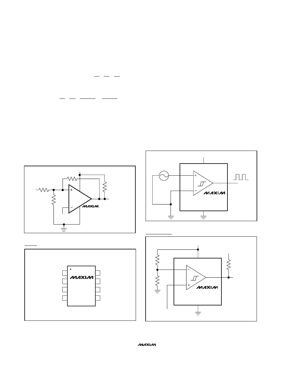
Figure 4. MAX918/MAX920 Additional Hysteresis
MAX919
IN+
OUT
V
CC
100mVp-p
V
CC
V
EE
IN-
Figure 5. Zero-Crossing Detector
Typical Application Circuit
OUT
N.C.
( ) ARE FOR MAX917/MAX918.
V
EE
1
2
8
7
N.C.
V
CC
IN- (REF)
IN+
N.C.
SO
TOP VIEW
3
4
6
5
MAX917
MAX918
MAX919
MAX920
Pin Configurations (continued)
6) Verify the trip voltages and hysteresis as follows:
Hysteresis = V
THR
- V
THF
Board Layout and Bypassing
Power-supply bypass capacitors are not typically
needed, but use 100nF bypass capacitors close to the
device’s supply pins when supply impedance is high,
supply leads are long, or excessive noise is expected
on the supply lines. Minimize signal trace lengths to
reduce stray capacitance. A ground plane and sur-
face-mount components are recommended.
Zero-Crossing Detector
Figure 5 shows a zero-crossing detector application.
The MAX919’s inverting input is connected to ground,
and its noninverting input is connected to a 100mVp-p
signal source. As the signal at the noninverting input
crosses 0V, the comparator’s output changes state.
Logic-Level Translator
The
Typical Application Circuit
shows an application
that converts 5V logic to 3V logic levels. The MAX920 is
powered by the +5V supply voltage, and the pull-up
resistor for the MAX920’s open-drain output is connect-
ed to the +3V supply voltage. This configuration allows
the full 5V logic swing without creating overvoltage on
the 3V logic inputs. For 3V to 5V logic-level translations,
simply connect the +3V supply voltage to V
CC
and the
+5V supply voltage to the pull-up resistor.
V rising: V
V
R1
1
R1
1
R2
1
R3
V falling: V
IN
THR
REF
IN
THF
=
+
+
=
⋅
V
R1
1
R1
1
R2
1
R3 R4
R1
R3 R4
V
REF
CC
+
+
+
−
+
⋅
⋅