Pin description – Rainbow Electronics MAX1494 User Manual
Page 8
MAX1492/MAX1494
3.5- and 4.5-Digit, Single-Chip ADCs
with LCD Drivers
8
_______________________________________________________________________________________
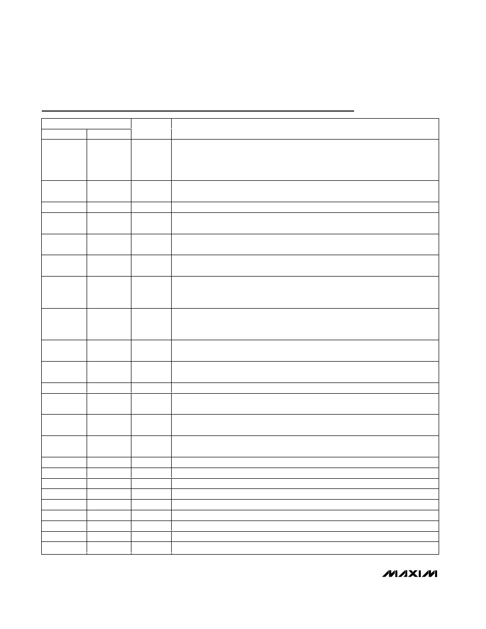
Pin Description
PIN
MAX1492
MAX1494
NAME
FUNCTION
1
30
CLK
External Clock Input. When the EXTCLK bit in the control register is set, CLK is the
master clock input for the modulator and the filter (frequency = 4.9152MHz). When the
EXTCLK bit in the control register is reset, the internal clock is used. Connect CLK to
GND or DV
DD
when the internal oscillator is used.
2
31
DV
DD
Digital Power Input. Connect DV
DD
to a 2.7V to 5.25V power supply. Bypass DV
DD
to
GND with 0.1µF and 4.7µF capacitors.
3
32
GND
Ground
4
1
AV
DD
Analog Power Input. Connect AV
DD
to a 2.7V to 5.25V power supply. Bypass AV
DD
to
GND with 0.1µF and 4.7µF capacitors.
5
2
AIN+
Positive Analog Input. Positive side of fully differential analog input. Bypass AIN+ to
GND with a 0.1µF or greater capacitor.
6
3
AIN-
Negative Analog Input. Negative side of fully differential analog input. Bypass AIN- to
GND with a 0.1µF or greater capacitor.
7
4
REF-
Negative Reference Input. During internal reference operation, connect REF- to GND.
For external reference operation, bypass REF- to GND with a 0.1µF capacitor and set
V
REF-
from -2.2V to +2.2V, provided V
REF+
> V
REF-
.
8
5
REF+
Positive Reference Input. During internal reference operation, connect a 4.7µF capacitor
from REF+ to GND. For external reference operation, bypass REF+ to GND with a 0.1µF
capacitor and set V
REF+
from -2.2V to +2.2V, provided V
REF+
> V
REF-
.
9
6
LOWBATT
Low-Battery Input. When V
LOWBATT
< 2.048V (typ), the LOWBATT symbol on LCD turns
on and the LOWBATT bit latches high in the status register.
10
7
EOC
Active-Low, End-of-Conversion Logic Output. A logic-low at EOC indicates that a new
ADC result is available in the ADC result register.
11
8
CS
Active-Low Chip-Select Input. Forcing CS low activates the serial interface.
12
9
DIN
Serial Data Input. Data present at DIN is shifted into the internal registers in response to
a rising edge at SCLK when CS is low.
13
10
SCLK
Serial Clock Input. Apply an external clock to SCLK to facilitate communication through
the serial bus. SCLK can idle high or low.
14
11
DOUT
Serial Data Output. DOUT presents serial data in response to register queries. Data
shifts out on the falling edge of SCLK. DOUT goes high impedance when CS is high.
15
12
SEG1
LCD Segment 1 Driver
16
13
SEG2
LCD Segment 2 Driver
17
14
SEG3
LCD Segment 3 Driver
18
15
SEG4
LCD Segment 4 Driver
19
16
SEG5
LCD Segment 5 Driver
20
17
SEG6
LCD Segment 6 Driver
21
18
SEG7
LCD Segment 7 Driver
22
19
SEG8
LCD Segment 8 Driver
23
20
SEG9
LCD Segment 9 Driver