Rainbow Electronics MAX1494 User Manual
Page 27
MAX1492/MAX1494
3.5- and 4.5-Digit, Single-Chip ADCs
with LCD Drivers
______________________________________________________________________________________
27
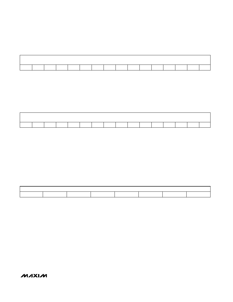
Default values: 0000h
The peak data register is a 16-bit read-only register.
Set the PEAK bit to 1 to enable the PEAK function. This
register stores the peak value of the ADC conversion
result. First, the current ADC result is saved to the
PEAK register. Then, the new ADC conversion result is
compared to this value. If the new value is larger than
the value in the peak register, the MAX1492/MAX1494
save the new value to the peak register. If the new
value is less than the value in the peak register,
the value in the peak register remains unchanged. Set
the PEAK bit to 0 to clear the value in the PEAK regis-
ter. The peak function is only valid for the range of
-19,487 to +19,999 for the MAX1494 and -1217 to
+1999 for the MAX1492.
The data is represented in two’s complement format.
For the MAX1494, the data is 16-bit and D15 is the MSB.
For the MAX1492, the data is 12-bit, D15 is the MSB, and
D4 is the LSB followed by four trailing sub-bits.
Default values: 0000h
The LCD data register is a 16-bit read/write register.
This register updates from the ADC result register 1, the
PEAK register, or from the serial interface by selecting
SPI/ADC bit, PEAK bit, and HOLD bit in the control reg-
ister (see Table 6). The data is represented in two’s
complement format.
For the MAX1494, the data is 16-bit and D15 is the MSB.
For the MAX1492, the data is 12-bit, D15 is the MSB,
and D4 is the LSB, followed by four trailing sub-bits.
MSB
LSB
(MAX1492)
LSB
(MAX1494)
D15
D14
D13
D12
D11
D10
D9
D8
D7
D6
D5
D4
D3
D2
D1
D0
MSB
LSB
(MAX1492)
LSB
(MAX1494)
D15
D14
D13
D12
D11
D10
D9
D8
D7
D6
D5
D4
D3
D2
D1
D0
MSB
LSB
D3
D2
D1
D0
0
0
0
0
Default values: 00h
The ADC result-register 2 is an 8-bit read-only register.
This register stores the 4 LSBs of the ADC result. Use
this result with the result in ADC result-register 1 to form
a 20-bit two’s complement conversion result.
LCD Data Register (Read/Write):
PEAK Register (Read Only):
ADC Result-Register 2 (Read Only):