Rainbow Electronics MAX1494 User Manual
Page 26
MAX1492/MAX1494
3.5- and 4.5-Digit, Single-Chip ADCs
with LCD Drivers
26
______________________________________________________________________________________
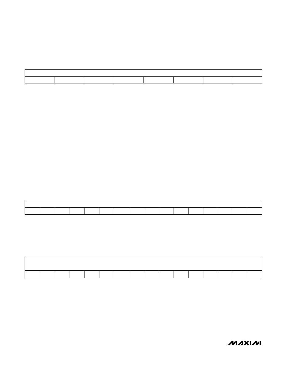
Default values: 00h
The LCD segment-display register 3 is an 8-bit
read/write register. When the SEG-SEL bit (in the con-
trol register) is set to 1, the MAX1492/MAX1494 provide
direct access to individual LCD segments. The bits in
the LCD segment-display register determine if a seg-
ment is on or off. Write a 0 to turn on a segment and a 1
to turn off a segment.
MSB
LSB
PEAK
HOLD
BC_
B4
C4
A4
G4
D4
D4:
Segment d Driver Bit of Digit 4. The
default value turns on the LCD segment
(MAX1494 only).
G4:
Segment g Driver Bit of Digit 4. The
default value turns on the LCD segment
(MAX1494 only).
A4:
Segment a Driver Bit of Digit 4. The
default value turns on the LCD segment
(MAX1494 only).
C4:
Segment c Driver Bit of Digit 4. The
default value turns on the LCD segment
(MAX1494 only).
B4:
Segment b Driver Bit of Digit 4. The
default value turns on the LCD segment
(MAX1494 only).
BC_:
Segment bc_ Driver Bit. For the
MAX1494, this bit enables BC5. For the
MAX1492, this bit enables BC4. The
default value turns on the LCD segment.
HOLD:
HOLD-Sign Driver Bit. The default value
turns on the HOLD annunciator.
PEAK:
PEAK-Sign Driver Bit. The default value
turns on the PEAK annunciator.
Default values: 0000h
In addition to automatic offset calibration, the
MAX1492/MAX1494 offer a user-defined custom-offset
16-bit read/write register. The final result of the ADC
conversion is the input after autocalibration minus the
value in the custom offset. The custom offset value is
stored in this register. D15 is the MSB. The data is rep-
resented in two’s complement format.
MSB
LSB
D15
D14
D13
D12
D11
D10
D9
D8
D7
D6
D5
D4
D3
D2
D1
D0
Default values: 0000h
The ADC result-register 1 is a 16-bit read-only register.
This register stores the 16 MSBs of the ADC result. The
data is represented in two’s complement format.
For the MAX1494, the data is 16-bit and D15 is the
MSB. For the MAX1492, the data is 12-bit, D15 is the
MSB, and D4 is the LSB.
MSB
LSB
(MAX1492)
LSB
(MAX1494)
D15
D14
D13
D12
D11
D10
D9
D8
D7
D6
D5
D4
D3
D2
D1
D0
LCD Segment-Display Register 3 (Read/Write):
ADC Custom Offset-Calibration Register (Read/Write):
ADC Result-Register 1 (Read Only):