Table 6. lcd priority table – Rainbow Electronics MAX1494 User Manual
Page 24
MAX1492/MAX1494
3.5- and 4.5-Digit, Single-Chip ADCs
with LCD Drivers
24
______________________________________________________________________________________
Default values: 7CF0h (for MAX1492, +1999)
4E1Fh (for MAX1494, +19,999)
The overrange register is a 16-bit read/write register
(D15 is the MSB). When the conversion result exceeds
the value in the overrange register, the OVER bit in the
status register latches to 1. The LCD shows a 1 fol-
lowed by 4 dashes for the MAX1494 or a 1 followed by
3 dashes for the MAX1492 (see Table 4).
The data is represented in two’s complement format.
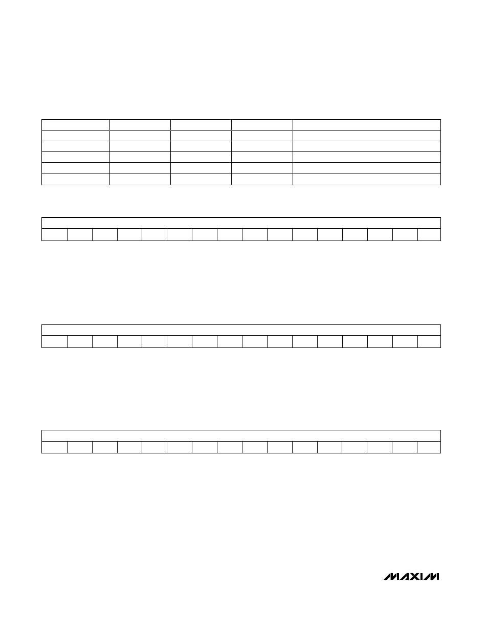
SEG_SEL
SPI/
ADC
HOLD
PEAK
DISPLAYS VALUES FROM
1
X
X
X
LCD Segment Registers
0
1
X
X
LCD Display Register (User Written)
0
0
1
X
LCD Display Register
0
0
0
1
Peak Register
0
0
0
0
ADC Result Register
Table 6. LCD Priority Table
X = Don’t care.
Underrange Register (Read/Write):
Overrange Register (Read/Write):
MSB
LSB
D15
D14
D13
D12
D11
D10
D9
D8
D7
D6
D5
D4
D3
D2
D1
D0
Default values: 8300h (for MAX1492, -2000)
B1E0h (for MAX1494, -20,000)
The underrange data register is 16-bit read/write regis-
ter (D15 is the MSB). When the conversion result falls
below the value in the underrange register, the UNDR
bit in the status register sets to 1. The LCD shows a -1
followed by 4 dashes for the MAX1494 or a -1 followed
by 3 dashes for the MAX1492 (see Table 4).
The data is represented in two’s complement format.
MSB
LSB
D15
D14
D13
D12
D11
D10
D9
D8
D7
D6
D5
D4
D3
D2
D1
D0
Default values: 0000h
The LCD segment-display register 1 is a 16-bit
read/write register. When the SEG-SEL bit (in the con-
trol register) is set to 1, the MAX1492/MAX1494 provide
direct access to individual LCD segments. The bits in
the LCD segment-display register determine if a seg-
ment is on or off. Write a 0 to this register to turn on a
segment and a 1 to turn off a segment.
MSB
LSB
A2
G2
D2
F2
E2
DP2
ANN
B1
C1
A1
G1
D1
F1
E1
DP1
0
LCD Segment-Display Register 1 (Read/Write):