Rainbow Electronics MAX1249 User Manual
Page 9
MAX1248/MAX1249
+2.7V to +5.25V, Low-Power, 4-Channel,
Serial 10-Bit ADCs in QSOP-16
_______________________________________________________________________________________
9
the acquisition time lengthens, and more time must be
allowed between conversions. The acquisition time,
t
ACQ
, is the maximum time the device takes to acquire
the signal, and is also the minimum time needed for the
signal to be acquired. It is calculated by:
t
ACQ
= 7.6 x (R
S
+ R
IN
) x 16pF
where R
IN
= 9k
Ω
, R
S
= the source impedance of the
input signal, and t
ACQ
is never less than 1.5µs. Note
that source impedances below 3k
Ω
do not significantly
affect the ADC’s AC performance.
Higher source impedances can be used if a 0.01µF
capacitor is connected to the individual analog inputs.
Note that the input capacitor forms an RC filter with the
input source impedance, limiting the ADC’s signal
bandwidth.
Input Bandwidth
The ADC’s input tracking circuitry has a 2.25MHz
small-signal bandwidth, so it is possible to digitize
high-speed transient events and measure periodic sig-
nals with bandwidths exceeding the ADC’s sampling
rate by using undersampling techniques. To avoid
high-frequency signals being aliased into the frequency
band of interest, anti-alias filtering is recommended.
Analog Input Protection
Internal protection diodes, which clamp the analog input
to V
DD
and AGND, allow the channel input pins to swing
from AGND - 0.3V to V
DD
+ 0.3V without damage.
However, for accurate conversions near full scale, the
inputs must not exceed V
DD
by more than 50mV or be
lower than AGND by 50mV.
If the analog input exceeds 50mV beyond the sup-
plies, do not forward bias the protection diodes of off
channels over 4mA.
How to Start a Conversion
A conversion is started by clocking a control byte into
DIN. With CS low, each rising edge on SCLK clocks a bit
from DIN into the MAX1248/MAX1249’s internal shift reg-
ister. After CS falls, the first arriving logic “1” bit defines
the control byte’s MSB. Until this first “start” bit arrives,
any number of logic “0” bits can be clocked into DIN with
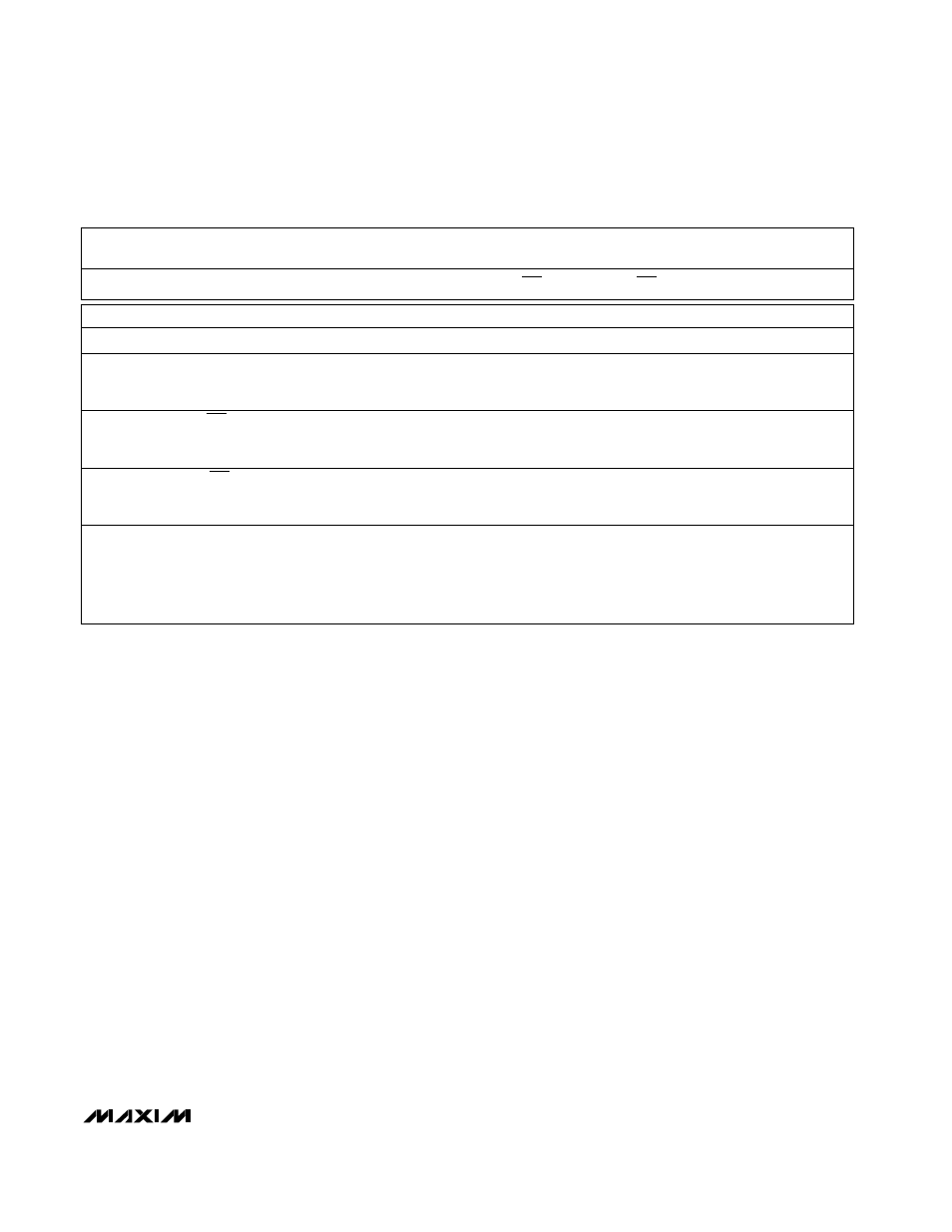
no effect. Table 1 shows the control-byte format.
The MAX1248/MAX1249 are compatible with SPI/QSPI
and MICROWIRE devices. For SPI, select the correct
clock polarity and sampling edge in the SPI control reg-
isters: set CPOL = 0 and CPHA = 0. MICROWIRE, SPI,
and QSPI all transmit a byte and receive a byte at the
same time. Using the
Typical Operating Circuit,
the sim-
Table 1. Control-Byte Format
BIT 7
BIT 6
BIT 5
BIT 4
BIT 3
BIT 2
BIT 1
BIT 0
(MSB)
(LSB)
START
SEL2
SEL1
SEL0
UNI/BIP
SGL/DIF
PD1
PD0
BIT
NAME
DESCRIPTION
7(MSB)
START
The first logic “1” bit after CS goes low defines the beginning of the control byte.
6
SEL2
These three bits select which of the four channels are used for the conversion (Tables 2 and 3).
5
SEL1
4
SEL0
3
UNI/BIP
1 = unipolar, 0 = bipolar. Selects unipolar or bipolar conversion mode. In unipolar mode, an
analog input signal from 0V to VREF can be converted; in bipolar mode, the signal can range
from -VREF / 2 to +VREF / 2.
2
SGL/DIF
1 = single ended, 0 = differential. Selects single-ended or differential conversions. In single-
ended mode, input signal voltages are referred to COM. In differential mode, the voltage
difference between two channels is measured (Tables 2 and 3).
1
PD1
Selects clock and power-down modes.
0(LSB)
PD0
PD1
PD0
Mode
0
0
Full power-down
0
1
Fast power-down (MAX1248 only)
1
0
Internal clock mode
1
1
External clock mode