Timing characteristics – Rainbow Electronics MAX1249 User Manual
Page 5
MAX1248/MAX1249
+2.7V to +5.25V, Low-Power, 4-Channel,
Serial 10-Bit ADCs in QSOP-16
_______________________________________________________________________________________
5
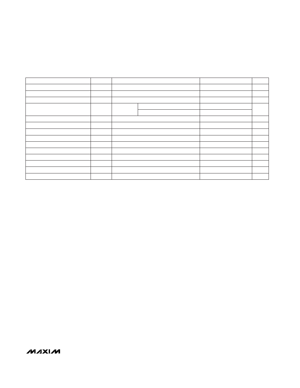
TIMING CHARACTERISTICS
(V
DD
= +2.7V to +5.25V, T
A
= T
MIN
to T
MAX
, unless otherwise noted.)
Note 1:
Tested at V
DD
= 2.7V; COM = 0V; unipolar single-ended input mode.
Note 2:
Relative accuracy is the deviation of the analog value at any code from its theoretical value after the full-scale range has
been calibrated.
Note 3:
MAX1248—internal reference, offset nulled; MAX1249 — external reference (VREF = +2.500V), offset nulled.
Note 4:
Ground “on” channel; sine wave applied to all “off” channels.
Note 5:
Conversion time defined as the number of clock cycles multiplied by the clock period; clock has 50% duty cycle.
Note 6:
The common-mode range for the analog inputs is from AGND to V
DD
.
Note 7
Sample tested to 0.1% AQL.
Note 8:
External load should not change during conversion for specified accuracy.
Note 9:
ADC performance is limited by the converter’s noise floor, typically 300µVp-p.
Note 10
Guaranteed by design. Not subject to production testing.
Note 11:
The MAX1249 typically draws 400
µ
A less than the values shown.
Note 12:
Measured as
|
V
FS
(2.7V) - V
FS
(5.25V)
|
.
DIN to SCLK Setup
ns
240
t
STR
CS Rise to SSTRB Output Disable
ns
240
t
SDV
CS Fall to SSTRB Output Enable
240
t
SSTRB
SCLK Fall to SSTRB
ns
200
t
CL
SCLK Pulse Width Low
ns
200
SCLK Pulse Width High
ns
0
CS to SCLK Rise Hold
ns
100
t
CSS
CS to SCLK Rise Setup
ns
240
t
TR
CS Rise to Output Disable
ns
240
t
DV
CS Fall to Output Enable
t
DO
SCLK Fall to Output Data Valid
ns
0
t
DH
DIN to SCLK Hold
ns
µs
1.5
t
ACQ
Acquisition Time
0
t
SCK
SSTRB Rise to SCLK Rise
ns
100
t
DS
UNITS
MIN
TYP
MAX
SYMBOL
PARAMETER
Internal clock mode only (Note 10)
External clock mode only, Figure 2
External clock mode only, Figure 1
Figure 1
Figure 2
Figure 1
CONDITIONS
ns
20
240
Figure 1
t
CSH
t
CH
ns
MAX124_ _C/E
MAX124_ _M
20
200