Table 7. full scale and zero scale, Layout, grounding, and bypassing, High-speed digital interfacing with qspi – Rainbow Electronics MAX1249 User Manual
Page 19
MAX1248/MAX1249
+2.7V to +5.25V, Low-Power, 4-Channel,
Serial 10-Bit ADCs in QSOP-16
______________________________________________________________________________________
19
UNIPOLAR MODE
BIPOLAR MODE
Full Scale
Zero Scale
Positive
Zero
Negative
Full Scale
Scale
Full Scale
VREF + COM
COM
VREF / 2
COM
-VREF / 2
+ COM
+ COM
011 . . . 111
011 . . . 110
000 . . . 010
000 . . . 001
000 . . . 000
111 . . . 111
111 . . . 110
111 . . . 101
100 . . . 001
100 . . . 000
- FS
COM*
OUTPUT CODE
ZS = COM
+FS - 1LSB
INPUT VOLTAGE (LSB)
+ COM
FS
=
VREF
2
-FS =
+ COM
-VREF
2
1LSB =
VREF
1024
*COM
≥
VREF / 2
+3V
+3V
GND
SUPPLIES
DGND
+3V
DGND
COM
AGND
V
DD
DIGITAL
CIRCUITRY
MAX1248
MAX1249
R* = 10
Ω
* OPTIONAL
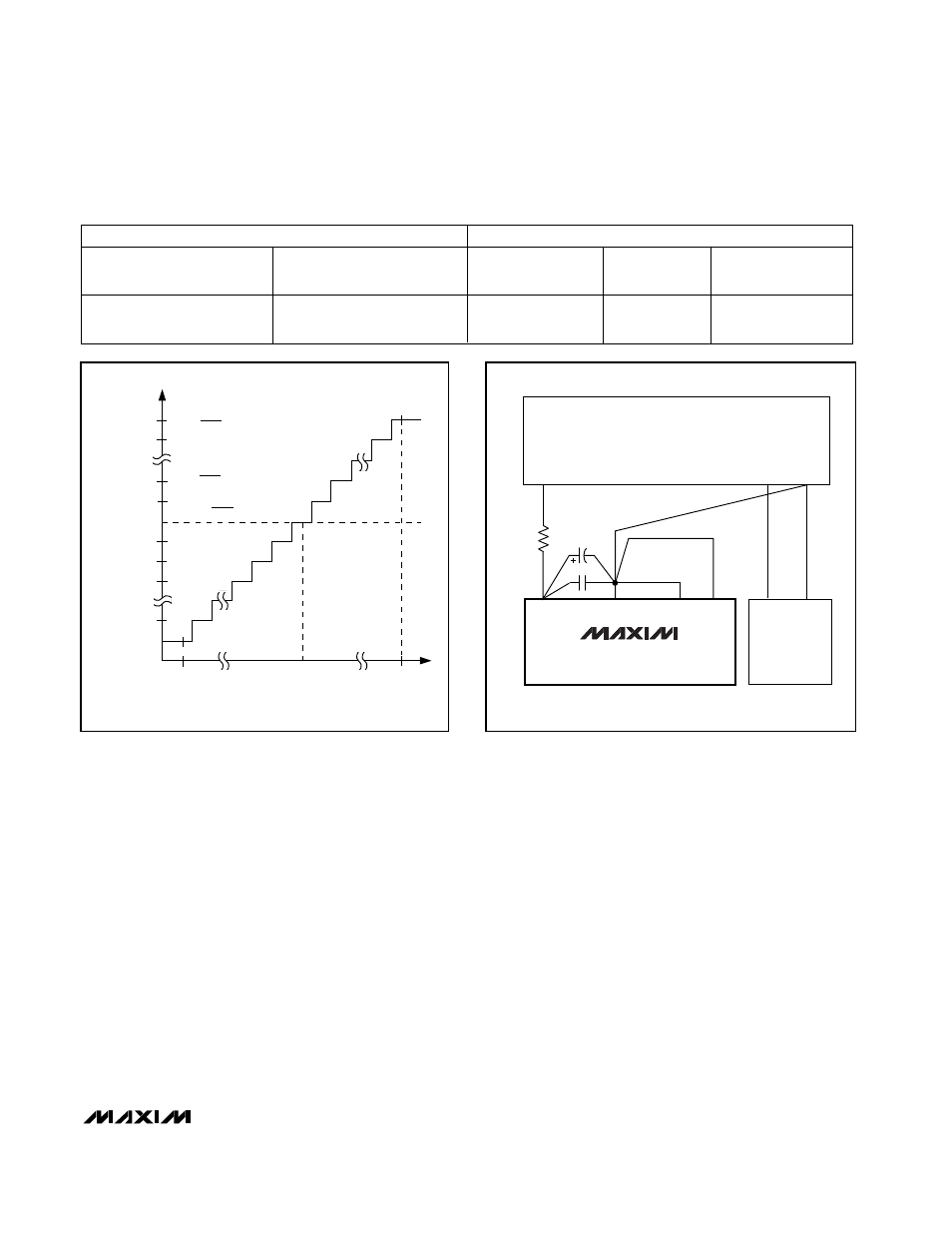
Figure 17. Bipolar Transfer Function, Zero Scale (ZS) = COM,
Full Scale (FS) = VREF / 2 + COM
Figure 18. Power-Supply Grounding Connection
Table 7. Full Scale and Zero Scale
Layout, Grounding, and Bypassing
For best performance, use printed circuit boards.
Wire-wrap boards are not recommended. Board layout
should ensure that digital and analog signal lines are
separated from each other. Do not run analog and digi-
tal (especially clock) lines parallel to one another, or
digital lines underneath the ADC package.
Figure 18 shows the recommended system ground
connections. Establish a single-point analog ground
(star ground point) at AGND, separate from the logic
ground. Connect all other analog grounds and DGND
to the star ground. No other digital system ground
should be connected to this ground. For lowest noise
operation, the ground return to the star ground’s power
supply should be low impedance and as short as pos-
sible.
High-frequency noise in the V
DD
power supply may
affect the ADC’s high-speed comparator. Bypass the
supply to the star ground with 0.1µF and 1µF capaci-
tors close to pin 1 of the MAX1248/MAX1249. Minimize
capacitor lead lengths for best supply-noise rejection.
If the +3V power supply is very noisy, a 10
Ω
resistor
can be connected as a lowpass filter (Figure 18).
High-Speed Digital Interfacing with QSPI
The MAX1248/MAX1249 can interface with QSPI using
the circuit in Figure 19 (f
SCLK
= 2.0MHz, CPOL = 0,
CPHA = 0). This QSPI circuit can be programmed to do a
conversion on each of the four channels. The result is
stored in memory without taxing the CPU, since QSPI
incorporates its own micro-sequencer.
The MAX1248/MAX1249 are QSPI compatible up to their
maximum external clock frequency of 2MHz.