Internal clock – Rainbow Electronics MAX1249 User Manual
Page 12
MAX1248/MAX1249
+2.7V to +5.25V, Low-Power, 4-Channel,
Serial 10-Bit ADCs in QSOP-16
12
______________________________________________________________________________________
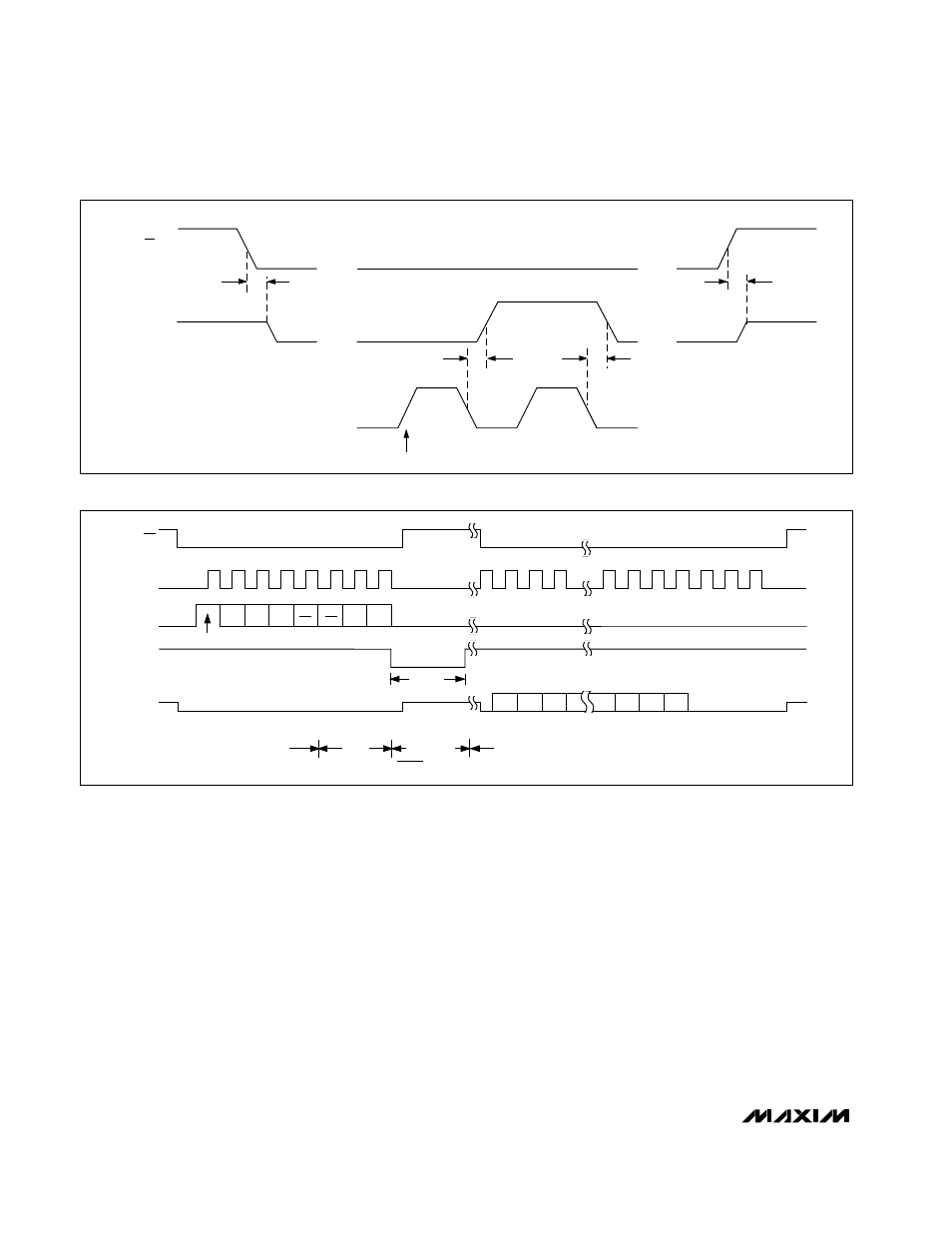
Internal Clock
In internal clock mode, the MAX1248/MAX1249 gener-
ate their own conversion clocks internally. This frees the
µP from the burden of running the SAR conversion clock
and allows the conversion results to be read back at the
processor’s convenience, at any clock rate from 0MHz
to 2MHz. SSTRB goes low at the start of the conversion
and then goes high when the conversion is complete.
SSTRB is low for a maximum of 7.5µs (SHDN = FLOAT),
during which time SCLK should remain low for best
noise performance.
An internal register stores data when the conversion is
in progress. SCLK clocks the data out of this register at
any time after the conversion is complete. After SSTRB
goes high, the next falling clock edge produces the
MSB of the conversion at DOUT, followed by the
remaining bits in MSB-first format (Figure 8). CS does
not need to be held low once a conversion is started.
Pulling CS high prevents data from being clocked into
the MAX1248/MAX1249 and three-states DOUT, but it
does not adversely affect an internal clock mode con-
version already in progress. When internal clock mode
is selected, SSTRB does not go into a high-impedance
state when CS goes high.
Figure 9 shows the SSTRB timing in internal clock
mode. In this mode, data can be shifted in and out of
the MAX1248/MAX1249 at clock rates exceeding
2.0MHz if the minimum acquisition time, t
ACQ
, is kept
above 1.5µs.
SSTRB
CS
SCLK
DIN
DOUT
1
4
8
12
18
20
24
START
SEL2 SEL1 SEL0
UNI/
BIP
SGL/
DIF
PD1 PD0
B9
MSB
B8
B7
B0
LSB
S1
S0
FILLED WITH
ZEROS
IDLE
CONVERSION
7.5µs MAX
(SHDN = FLOAT)
2
3
5
6
7
9
10
11
19
21
22
23
t
CONV
ACQUISITION
(f
SCLK
= 2MHz)
IDLE
A/D STATE
1.5µs
Figure 8. Internal Clock Mode Timing
• • •
• • •
• • •
• • •
t
SDV
t
SSTRB
PD0 CLOCKED IN
t
STR
SSTRB
SCLK
CS
t
SSTRB
• • •
• • • •
•
Figure 7. External Clock Mode SSTRB Detailed Timing